ASML Develops Virtual Metrology Technology for Semiconductor Manufacturing with Machine Learning
“As a process engineer I had no experience with neural networks or machine learning. I worked through the MATLAB examples to find the best machine learning functions for generating virtual metrology. I couldn’t have done this in C or Python—it would’ve taken too long to find, validate, and integrate the right packages.”
Challenge
Solution
Results
- Industry leadership established
- Potential manufacturing improvements identified
- Maintenance overhead minimized

In nanofabrication, photolithography is the fundamental patterning step that controls the size of a microchip. During photolithography, a low-wavelength power source is conditioned with optics through an image that is then reduced in size with more optics into a thin film of light-sensitive chemical covering a substrate, typically silicon. This step is repeated until all available surface area on the substrate has been exposed with the same image; the result is referred to as a layer. Multiple exposed layers are needed to create the complex microscopic structures that make up a chip. To prevent yield issues due to connection failures between layers, all patterns between layers must line up as intended.
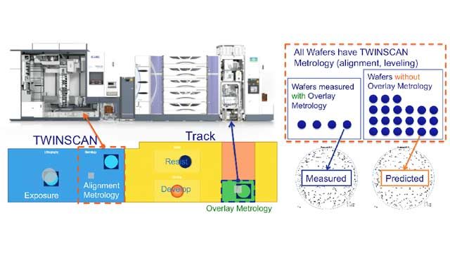
To ensure layer alignment without affecting throughput, ASML’s TWINSCAN photolithography system must limit the number of alignment marks it measures before the exposure step. The general rule is that the time required to measure alignment marks cannot be longer than the time required to expose the previous wafer in the sequence. Due to the large quantity of overlay marks required for a proper overlay model correction, it is not feasible to measure every wafer coming out of a TWINSCAN system.
ASML used MATLAB® and Statistics and Machine Learning Toolbox™ to develop virtual overlay metrology software. This software applies machine learning techniques to come up with a predicted estimate of overlay metrology for every wafer, using alignment metrology data.
“The work we’ve done with MATLAB and machine learning demonstrates industry leadership in the best use of existing metrology,” says Emil Schmitt-Weaver, applications development engineer at ASML. “The papers we’ve published on this work have attracted the interest of customers looking to improve their manufacturing processes with ASML products.”
Challenge
Because Schmitt-Weaver had no previous experience in developing machine learning algorithms, he decided not to develop the algorithms in Python, C, or another low-level language. He wanted to develop a prototype quickly, relying on functions that have been deployed across ASML’s large, diverse user base and maintained by dedicated professionals.
Solution
Schmitt-Weaver used MATLAB, Statistics and Machine Learning Toolbox, and Deep Learning Toolbox™ to develop a method for generating virtual metrology.
To start, Schmitt-Weaver used the Neural Network Time Series Prediction and Modeling app to learn how to prepare data for use with Deep Learning Toolbox. Using the app, he generated and exported the example code, which gave him a more detailed understanding of how the functions could be used together. As his competence increased, he was able to build on the generated code using examples from the vast multidisciplinary user community on MATLAB Central.
Schmitt-Weaver collected alignment metrology data from TWINSCAN systems and overlay metrology data from the same wafers using YieldStar systems. He then split the data set into two groups, one for training the network and one for validating it.
Using Deep Learning Toolbox and Statistics and Machine Learning Toolbox, he designed a nonlinear autoregressive network with exogenous inputs (NARX) and trained it with data from the training group.
To avoid overfitting the neural network to the training group, he used Deep Learning Toolbox to implement automated regularization with a Bayesian framework.
After the network was trained, he supplied it with input from the test data and verified its results against the measured results from the YieldStar system.
ASML used the data collected to develop a prototype real-time overlay controller in MATLAB. The network provided the foundation for potentially improving yield, as well as the ability to identify wafers that might not have received overlay metrology.
Results
Industry leadership established. “By using MATLAB to improve overlay metrology, we showed our customers that we are leaders in developing innovative ways to reach their overlay performance goals,” says Schmitt-Weaver.
Potential manufacturing improvements identified. “The network we designed and trained in MATLAB identified systematic and random overlay errors that might otherwise have gone undetected,” notes Schmitt-Weaver. “This degree of improvement to overlay performance is necessary for microchip fabrication up to and below the 5nm node.”
Maintenance overhead minimized. “Since the company’s beginnings, ASML systems have made use of compiled MATLAB algorithms,” says Schmitt-Weaver. “By building upon the large database of peer-reviewed legacy scripts, I was able to focus my attention on the new machine learning functionalities.”
"Virtual overlay metrology for fault detection supported with integrated metrology and machine learning," Proc. SPIE 9424, Metrology, Inspection, and Process Control for Microlithography XXIX, 94241T (March 19, 2015), doi:10.1117/12.2085475.