Modeling and Analysis of Probe-Fed Stacked Patch Antenna
This example shows the steps to model and analyze a probe-fed stacked patch antenna. The standard rectangular microstrip patch antenna has a narrow impedance bandwidth typically less than 5%. The stacked patch configuration is one of the ways of increasing the impedance bandwidth of these antennas to be greater than 25% [1]. There are different ways of designing stacked patches, primarily differing in the way their feed is designed [2]. The two types of feeding mechanisms are probe-feed and aperture coupled. These two mechanisms have a role in the impedance bandwidth behavior as well as the radiation characteristics of the antenna.
Probe-Fed Stacked Patch Geometry
The stacked patch comprises of two patches of slightly different sizes positioned over each other along the z-axis and separated by a dielectric material. Both patches are centered relative to the groundplane. The gap between the lower patch and the groundplane is also filled with a dielectric material. Either the top or the bottom patch is driven with a coaxial probe when used in a single feed configuration. A plan view of the geometry is shown in the sketch here.
Define Units
Define standard units for distance, frequency and resistance as well as their multiplicative equivalents for this example.
meter = 1;
hertz = 1;
ohm = 1;
mm = 1e-3*meter;
GHz = 1e9*hertz;
Antenna Dimensions
The antenna dimensions are provided in [1] for a probe-fed rectangular stacked patch with two substrate layers. The variables names are identical to those mentioned in [1] barring those of the groundplane. For this example, a square groundplane is chosen with size of three times the length of the top patch. The dimensions of the two patches are chosen to maximize the impedance bandwidth and guidelines are provided in [1] for designing such patch antennas together with a sensitivity analysis. For the geometry being modeled, the upper patch is slightly larger than the lower one.
L1 = 13.5*mm;
W1 = 12.5*mm;
L2 = 15*mm;
W2 = 16*mm;
d1 = 1.524*mm;
d2 = 2.5*mm;
xp = 5.4*mm;
r_0 = 0.325*mm;
Lgnd = 3*L2;
Wgnd = 3*L2;
Create Layer Shapes and Substrates
Layers: Use the rectangle shape from the catalog to create the three metal layers required for the stacked patch, namely for the upper patch, the lower patch and the groundplane. All the layers are centered about the coordinate axis origin. Plot the layer boundaries to confirm their sizes and positions.
pU = antenna.Rectangle(Length=L2,Width=W2);
pL = antenna.Rectangle(Length=L1,Width=W1);
pGnd = antenna.Rectangle(Length=Lgnd,Width=Wgnd);
figure
plot(pGnd)
hold on
plot(pU)
plot(pL)
grid on
legend('Groundplane','Upper patch','Lower patch',Location='best')
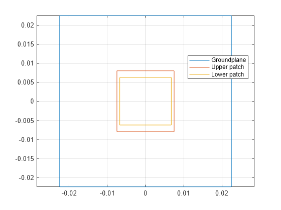
Dielectric Substrates: The stacked patch antenna in this example has a dielectric substrate between the upper and lower patches as well as between the lower patch and the groundplane. The lower patch has higher relative permittivity than the upper patch. This implies a loose electrical coupling between the two patches.
epsr_1 = 2.2;
tandelta_1 = 0.001;
dL = dielectric;
dL.Name = 'Lower sub';
dL.EpsilonR = epsr_1;
dL.LossTangent = tandelta_1;
dL.Thickness = d1;
epsr_2 = 1.07;
tandelta_2 = 0.001;
dU = dielectric;
dU.Name = 'Upper sub';
dU.EpsilonR = epsr_2;
dU.LossTangent = tandelta_2;
dU.Thickness = d2;Create Stacked Patch Model
Create the stacked patch antenna model by using pcbStack. Assign the layers starting from the top-most layer, in this case the metal layer for the upper patch and proceed to the lowest layer which is the groundplane. The probe-feed is specified between the lower patch and the ground plane. To improve the accuracy of the model, we switch the feed model to be a solid column approximated to a square shape. The default feed model is a strip wherein the strip approximation to a cylinder is used.
p = pcbStack;
p.Name = 'Stacked patch - Waterhouse';
p.BoardShape = pGnd;
p.BoardThickness = d1+d2;
p.Layers = {pU,dU,pL,dL,pGnd};
p.FeedLocations = [xp 0 3 5];
p.FeedDiameter = 2*r_0;
p.FeedViaModel = 'square';
figure
show(p)

Impedance Analysis
Analyze the stacked patch impedance over the frequency range 6-9 GHz. The stacked patch structure over this range should show two closely spaced parallel resonances. Prior to analysis, mesh the structure
fmax = 9*GHz;
fmin = 6*GHz;
deltaf = 0.125*GHz;
freq = fmin:deltaf:fmax;
mesh(p,MaxEdgeLength=0.01,MinEdgeLength=0.003)

figure
impedance(p,freq)

Stacked Patch Mesh
The impedance analysis over the frequency range 6 - 9 GHz, results in automatic mesh generation at the highest frequency. The mesh consists of triangles, which discretize all metal surfaces of the antenna and tetrahedra, which discretize the volume of the dielectric substrates. Plot the mesh for the metal surfaces and dielectric surfaces.
figure
mesh(p,view='metal')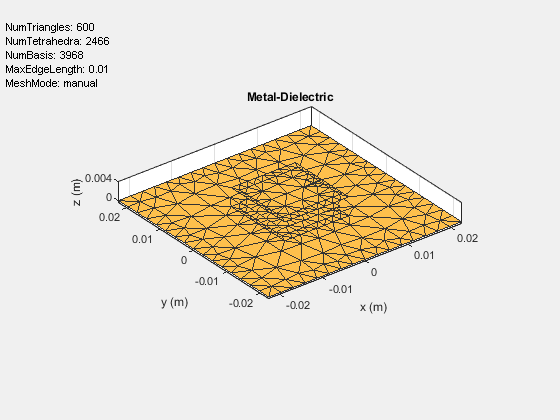
figure
mesh(p,view='dielectric surface')
Note that a column feed model with square shaped side walls approximating a cylindrical feed is used in this patch antenna. Use the metal mesh to get a closer view of this feed structure.
Reflection Coefficient
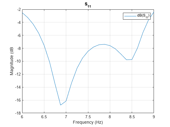
Since the antenna is excited by a coaxial probe, calculate the reflection coefficient at the input relative to 50-ohm reference impedance.
Zref = 50*ohm;
s = sparameters(p,freq,Zref);
figure
rfplot(s,1,1)
title('S_1_1')
xlabel('Frequency (Hz)')
ylabel('Magnitude (dB')
figure
smplot = smithplot(s);
smplot.TitleTop = 'Input Reflection Coefficient';
smplot.LineWidth = 3;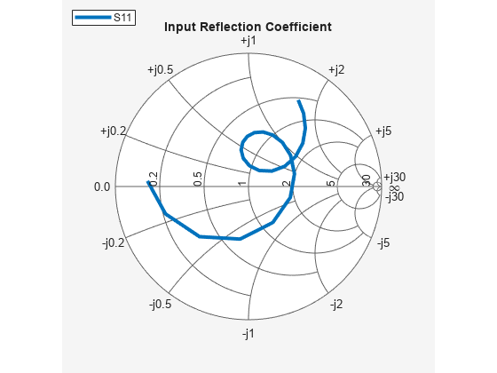
The results for the reflection coefficient match very well with the experiment results reported in [1]. The presence of the double resonance in the impedance behavior, has implications on the radiation pattern behavior of the antenna.
Pattern Variations Across Band
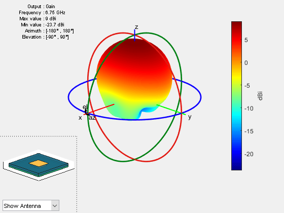
The wide impedance bandwidth observed from the port analysis of the stacked patch will have an impact on the far-field radiation pattern. To understand this, plot the radiation pattern in the far-field of this antenna at the 2 notches in the reflection coefficient plot - 6.75 GHz and 8.25 GHz.
patternfreqs = [6.75*GHz, 8.25*GHz];
freqIndx = arrayfun(@(x) find(freq==x),patternfreqs);
figure
pattern(p,freq(freqIndx(1)))
figure
pattern(p,freq(freqIndx(2)))

Realized Gain Variation Across Band
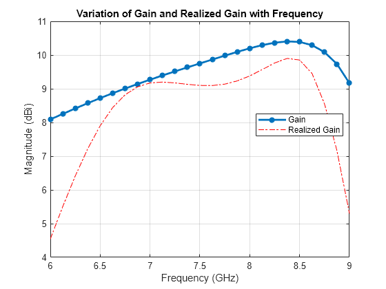
The pattern is relatively stable at higher elevation angles close to zenith. However, note that the radiation towards the horizon and backlobe seems to grow at the higher frequency end of the 6-9 GHz band. These results account for the losses in the dielectric but not for the impedance mismatches that might exist at the feed point. To understand the effect of the impedance mismatch, calculate the realized gain at zenith and compare it with the gain.
D = zeros(1,numel(freq));
az = 0;
el = 90;
for i = 1:numel(freq)
    D(i) = pattern(p,freq(i),az,el);
end
Plot Gain
h = figure;
plot(freq./GHz,D,'-*',LineWidth=2)
xlabel('Frequency (GHz)')
ylabel('Magnitude (dBi)')
grid on
title('Gain Variation With Frequency')

Calculate mismatch factor
gamma = rfparam(s,1,1);
mismatchFactor = 10*log10(1 - abs(gamma).^2);
Compute Realized Gain
Gr = mismatchFactor.' + D;
figure(h)
hold on
plot(freq./GHz,Gr,'r-.')
legend('Gain','Realized Gain',Location='best')
title('Variation of Gain and Realized Gain with Frequency')
hold off
Summary
The experimental results of the stacked patch design reported in [1] agree well with the analysis results shown in this example. In addition the antenna exhibits good stability in gain variation close to zenith with higher variations in shape near the horizon and the backlobe regions. The maximum realized gain at zenith is achieved at the lower and upper frequency ends of the 6 - 9 GHz band, especially at the notches in the input reflection coefficient where the match is the best. Within the 7 - 9 GHz range observe that the realized gain only drops off by about 0.6 dB. The reduced values of the realized gain below 6.5 GHz and above 8.5 GHz are due to the impedance mismatch.
References
[1] R. B. Waterhouse, "Design of probe-fed stacked patches," in IEEE Transactions on Antennas and Propagation, vol. 47, no. 12, pp. 1780-1784, Dec 1999.
[2] D.Orban and G.J.K.Moernaut, The Basics of Patch Antennas, Updated, Orban Microwave Products.
[3] C. A. Balanis, 'Antenna Theory. Analysis and Design,' p.514, Wiley, New York, 3rd Edition, 2005