System Timing
In the generated Software Interface Model obtained in the Hardware-Software Co-Design Workflow, you can set the schedule tick event that starts the loop running the software on the ARM® processor. The order of operations in the loop depends on the Simulink® sorted execution order. See Control and Display Execution Order (Simulink).
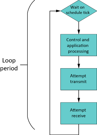
The following representative loop applies to a transmission and reception pair.

Configure the model so that the entire loop can run within the model base rate. You can determine the model base rate by your choice of scheduler and by specifying the frame sizes and rates of the transmitter and receiver blocks.
Keep the relationships between rates in your model simple. Simulink generates software to run the main loop at the common base period of your system. It uses subrates to achieve the other rates specified in your software model. If you specify rates with complex relationships, Simulink can calculate a base rate so small that completing the loop within the loop period becomes impossible.
The model must complete algorithmic or control operations within the frame period to prevent inhibiting the reception or transmission of further data. If the model misses a transmit or receive slot, it drops frames, resulting in lost samples or gaps in transmission. When the model contains transmit and receive blocks that run at different rates, operation scheduling can become especially problematic.
To reduce the frame rate and the amount of context switching on the ARM, you can specify larger frame sizes and lower baseband sample rates. However, these changes can cause heavier processing loads. If the resulting loads are unacceptable, try moving parts of the software model from the ARM into the FPGA user logic or implementing the model more efficiently.
As a best practice, try to keep the frame rate under 5 kHz.
The remaining sections describe the major steps in the loop.
Wait On Schedule Tick
First, the ARM software waits on the schedule tick, or loop trigger.
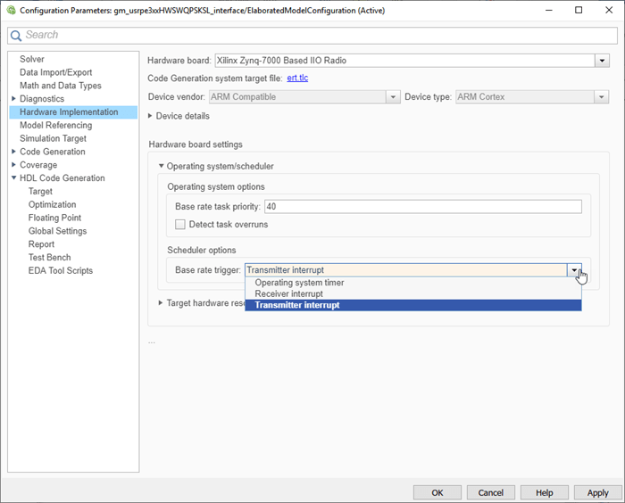
Select a loop trigger as required by your specific application. In the model configuration parameters for the model:
Select the Hardware Implementation pane.
Set the Hardware board parameter to
Xilinx Zynq-7000 Based IIO
                     Radio
for any of these target platforms:E310
E312
Select a Base rate trigger setting:
Operating system timer— The loop trigger is a timer tick at the base rate, which you configure as the smallest sample time in the system. Configure the other rates in the model as integer multiples of the sample time.Receiver interrupt— The loop trigger is an interrupt that occurs when a frame becomes available for reading from the receive user logic on the FPGA. The fastest rate in the model must be the sample time at the output port of the Receiver block. Configure the other rates in the model as integer multiples of this sample time.Transmitter interrupt— The loop trigger is an interrupt that occurs when a frame is available for writing to the user logic on the FPGA. The fastest rate in the model must be the sample time at the input port of the Transmitter block. Configure the other rates in the model as integer multiples of this sample time.

Control and Application Processing
In this step, the ARM software carries out processing that does not require data transmission or reception. Such processing includes accessing AXI registers on the user logic and other processing in the model, such as generating and consuming streaming data.
Attempt Transmit
In a transmission attempt, the ARM software sends a frame of data to the user logic on the FPGA. The input port to the block determines the frame size and frame rate. The transmitter hardware transmits the frame at the baseband sample rate that you entered in the Transmitter block dialog box.

To send a new frame, the software:
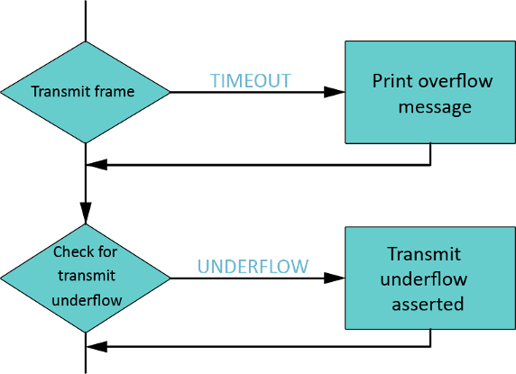
Checks for a free buffer in which to send a frame to the FPGA.
If a frame can be sent, the software sends the new frame to the FPGA and continues.
If a frame cannot be sent, the software waits for the time specified in the transmitter timeout block parameter.
If the timeout time passes and the frame has not been sent, the software discards the new frame, prints an overflow message, and continues.
If the software detects a gap in the data stream between the ARM processor and the user logic, the software asserts the underflow port.
To cause the software to wait indefinitely, in the Transmitter block,
set the Data timeout (sec) parameter to Inf. To
cause the software to return immediately without blocking, set the value to
0. The default value is Inf.
The base rate trigger setting determines the transmission rate:
Transmitter interrupt— The model runs at the rate at which the FPGA can accept frames of data from the ARM. This rate is directly linked to the baseband sample rate configured on the RF card. Under normal operation, overflows do not occur because the transmitter interrupt occurs when a frame buffer becomes available. For this setting type, the transmitter timeout does nothing.Receiver interrupt— The model runs at the rate at which frames of data arrive at the ARM from the FPGA. Configure the transmitter to generate data at this rate or at an integer multiple of this rate. The transmitter timeout determines how long the software waits for a transmit buffer to become available.Operating system timer— Configure the model so that it runs at the rate at which the user logic on the FPGA consumes data. If the rate of FPGA consumption and the rate of ARM generation do not match, use the timeout value to synchronize the two rates. Set the input frame rate to a value that is consistent with the rate changes designed into the user logic. Suppose the input frame size is N and the baseband sample rate is F. If the user logic upsamples internally by a factor of L to attain this sample rate, scale the input frame period by L:L * N / F
Attempt Receive
In a receive attempt, the ARM software receives a frame of data from the user logic on the FPGA. To specify the required frame size, use the Samples per frame parameter on the Receive block. The ARM Frame Rate signal specification block determines the frame rate.

To receive a frame from the FPGA, the software:
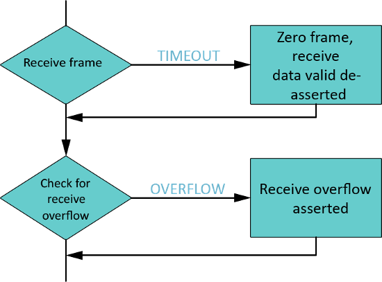
Checks for an available frame of data.
If a full frame is ready, the software receives the data and asserts the
data validport.If a full frame is not ready, the software waits for the time specified in the receiver timeout parameter.
If the timeout time passes and the data is still not ready, the processor outputs an invalid frame consisting of zeros, de-asserts the data valid port, and continues.
If the software has not consumed data coming from the FPGA, the software asserts the overflow port.
To cause the software to wait indefinitely, in the Receiver block, set the
Data timeout (sec) parameter to Inf. To cause
the software to return immediately without blocking, set the value to
0. The default value is Inf.
The base rate trigger setting type determines the reception rate:
Receiver interrupt— The model runs at the rate at which frames of data arrive at the ARM from the FPGA. This rate is directly linked to the baseband sample rate configured on the RF card and the valid data modeling within the user logic. Under normal operation, receiver timeouts do not happen because the receiver interrupt occurs only when a frame of data is available. For this setting type, the receiver timeout does nothing.Transmitter interrupt— The model runs at the rate at which the FPGA can accept frames of data from the ARM. Configure the receiver to consume data at this rate or at an integer multiple of this rate. The receiver timeout determines how long the software waits for a frame of data to become available.Operating system timer— Configure the model to receive and process data at the rate at which the user logic generates data. If the rate of FPGA consumption and the rate of ARM generation do not match, use the timeout value to synchronize the two rates. Set the output frame rate to a value that is consistent with the rate changes designed into the user logic. Suppose that the output frame size is N and the baseband sample rate is F. If the user logic downsamples internally by a factor of M to attain this sample rate, scale the output frame period by M:M * N / F