QPSK Receiver with USRP Hardware in Simulink
This model shows how to use the Universal Software Radio Peripheral™ (USRP) device with Simulink® to implement a QPSK receiver. The receiver addresses practical issues in wireless communications, e.g. carrier frequency and phase offset, timing offset and frame synchronization. This model receives the signal sent by the QPSK Transmitter with USRP Hardware in Simulink example at bit rate of 1 Mbps. The receiver demodulates the received symbols and outputs a simple message to the MATLAB® command line.
In order to run this model, you need to ensure that the specified center frequency of the USRP Receiver is within the acceptable range of your USRP daughter board.
Required Hardware and Software
To run this example, you will need one of the following hardware and the corresponding software support package.
USRP N2xx or B2xx series radio and Communications Toolbox Support Package for USRP Radio. For information on supported radios, see Supported Hardware and Required Software.
USRP E3xx, N3xx, X3xx, or X4xx series radio and Wireless Testbench Support Package for NI USRP Radios. For information on supported radios, see Supported Radio Devices (Wireless Testbench).
Overview
This model performs all processing at complex baseband to handle a time-varying frequency offset, a time-varying symbol delay, and Gaussian noise. To cope with the above-mentioned impairments, this example provides a reference design of a practical digital receiver, which includes correlation-based coarse frequency compensation, symbol timing recovery with fixed-rate resampling and bit stuffing/skipping, fine frequency compensation, frame synchronization and phase ambiguity resolution. The example uses some key algorithms in MATLAB, emphasizing textual algorithm expression over graphical algorithm expression.
Structure of the Example
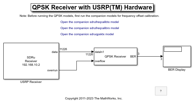
The top-level structure of the model is shown in the following figure. Which includes a USRP receiver block, a QPSK Receiver subsystem and a BER Display blocks.

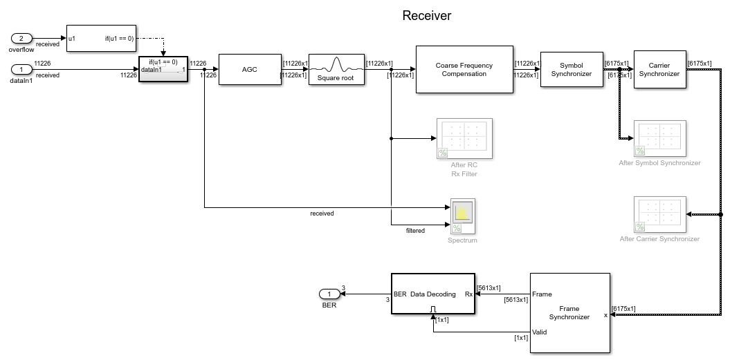
The detailed structures of the QPSK Receiver subsystem are illustrated in the following figure.

The components are further described in the following sections.
AGC - Automatic gain control
Raised Cosine Receive Filter - Uses a rolloff factor of 0.5
Coarse Frequency Compensation - Estimates an approximate frequency offset of the received signal and corrects it
Symbol Synchronizer - Resamples the input signal according to a recovered timing strobe so that symbol decisions are made at the optimum sampling instants
Carrier Synchronizer - Compensates for the residual frequency offset and the phase offset
Preamble Detector - Detect location of the frame header
Frame Synchronizer - Aligns the frame boundaries at the known frame header
Data Decoding - Resolves the phase ambiguity caused by the Carrier Synchronizer, demodulates the signal, and decodes the text message
Receiver
AGC
The received signal amplitude affects the accuracy of the carrier and symbol synchronizer. Therefore the signal amplitude should be stabilized to ensure an optimum loop design. The AGC output power is set to a value ensuring that the equivalent gains of the phase and timing error detectors keep constant over time. The AGC is placed before the Raised Cosine Receive Filter so that the signal amplitude can be measured with an oversampling factor of two, thus improving the accuracy of the estimate. You can refer to Chapter 7.2.2 and Chapter 8.4.1 of [ 1 ] for details on how to design the phase detector gain.
Raised Cosine Receive Filter
The Raised Cosine Receive Filter provides matched filtering for the transmitted waveform with a rolloff factor of 0.5.
Coarse Frequency Compensation
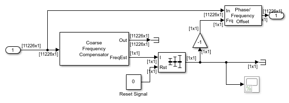
The Coarse Frequency Compensation subsystem corrects the input signal with a rough estimate of the frequency offset. The following diagram shows the subsystem, in which the frequency offset is estimated by averaging the output of the correlation-based algorithm of the Coarse Frequency Compensator block. The compensation is performed by the Phase/Frequency Offset block. There is usually a residual frequency offset even after the coarse frequency compensation, which would cause a slow rotation of the constellation. The Carrier Synchronizer block compensates for this residual frequency.
The accuracy of the Coarse Frequency Compensator decreases with its maximum frequency offset value. Ideally, this value should be set just above the expected frequency offset range.

Symbol Synchronizer
The timing recovery is performed by a Symbol Synchronizer library block, which implements a PLL, described in Chapter 8 of [ 1 ], to correct the timing error in the received signal. The timing error detector is estimated using the Gardner algorithm, which is rotationally invariant. In other words, this algorithm can be used before or after frequency offset compensation. The input to the block is oversampled by two. On average, the block generates one output symbol for every two input samples. However, when the channel timing error (delay) reaches symbol boundaries, there will be one extra or missing symbol in the output frame. In that case, the block implements bit stuffing/skipping and generates one more or less samples comparing to the desired frame size. So the output of this block is a variable-size signal.
The Damping factor, Normalized loop bandwidth, and Detector gain parameters of the block are tunable. Their default values are set to 1 (critical damping), 0.01 and 5.4 respectively, so that the PLL quickly locks to the correct timing while introducing little timing jitter.
Carrier Synchronizer
The fine frequency compensation is performed by a Carrier Synchronizer library block, which implements a phase-locked loop (PLL), described in Chapter 7 of [ 1 ], to track the residual frequency offset and the phase offset in the input signal. The PLL uses a Direct Digital Synthesizer (DDS) to generate the compensating phase that offsets the residual frequency and phase offsets. The phase offset estimate from DDS is the integral of the phase error output of a Loop Filter.
The Damping factor and Normalized loop bandwidth parameters of the block are tunable. Their default values are set to 1 (critical damping) and 0.01 respectively, so that the PLL quickly locks to the intended phase while introducing little phase noise.
Frame Synchronizer
The preamble detection and frame synchronization is performed by a MATLAB System block using a FrameSynchronizer System object. The Preamble Detector uses the known frame header (QPSK-modulated Barker code) to correlate against the received QPSK symbols in order to find the location of the frame header. The Frame Synchronizer block uses this location information to align the frame boundaries. It also transforms the variable-size output of the Symbol Synchronizer block into a fixed-size frame, which is necessary for the downstream processing. The second output of the block is a Boolean scalar indicating if the first output is a valid frame with the desired header and if so, enables the Data Decoding subsystem to run.
Data Decoding
The Data Decoding enabled subsystem performs phase ambiguity resolution, demodulation and text message decoding. The Carrier Synchronizer block may lock to the unmodulated carrier with a phase shift of 0, 90, 180, or 270 degrees, which can cause a phase ambiguity. For details of phase ambiguity and its resolution, please refer to Chapter 7.2.2 and 7.7 in [ 1 ]. The Phase Offset Estimator subsystem determines this phase shift. The Phase Ambiguity Correction & Demodulation subsystem rotates the input signal by the estimated phase offset and demodulates the corrected data. The payload bits are descrambled, and then decoded. All of the stored bits are converted to characters are printed in the Simulink Diagnostic Viewer.

Running the Example
Before running this model, first start the sdruqpsktx.slx QPSK Transmitter with USRP Hardware model.
This receiver model is capable of handling a frequency offset of 12.5kHz between the transmitter and receiver boards. However, when the frequency offset exceeds this range, the Coarse Frequency Compensation subsystem cannot accurately determine the offset of the received signal, which is critical for correct timing recovery and data decoding. We encourage you to run the companion frequency calibration sdrufreqcalib.slx transmitter and sdrufreqcalib_rx.slx receiver models with your USRP transmitter and receiver hardware to roughly determine the frequency offset between your two USRP boards. With that frequency offset value, you can manually adjust the Center frequency of the USRP Receiver subsystem in the receiver model to ensure a residual frequency offset that the model can track.
If the received signal is too weak or too strong, you might notice some garbled message output. In that case, you can change the gain of either the USRP Transmitter subsystem in the sdruqpsktx.slx QPSK Transmitter with USRP Hardware model or the USRP Receiver subsystem in the current model for better reception. Please also change the preamble detector threshold, in case you may see some recurrent garbled message output. This is because when the threshold of the preamble detector is set too low, the following steps will try to decode the header. When the threshold is set too high, you may not getting any outputs.
To run this model, first turn on the USRP hardware and connect it to the computer. Set the Center frequency parameter of the USRP Receiver block according to the center frequency setting of the sdruqpsktx.slx QPSK Transmitter with USRP Hardware model and the frequency calibration result. Then run the model. To ensure real-time processing, the model is by default set to run in Accelerator mode, and to remove all signal visualization. The received messages are decoded and printed out in the View diagnostics window while the simulation is running.
Exploring the Example
The example allows you to experiment with multiple system capabilities to examine their effect on bit error rate performance.
You can tune the Normalized loop bandwidth and Damping factor parameters of the Symbol Synchronizer and Carrier Synchronizer blocks, to assess their convergence time and estimation accuracy. In addition, you can assess the pull-in range of the Carrier Synchronizer block. With a large Normalized loop bandwidth and Damping factor, the PLL can acquire over a greater frequency offset range. However a large Normalized loop bandwidth allows more noise, which leads to a large mean squared error in the phase estimation. "Underdamped systems (with Damping Factor less than one) have a fast settling time, but exhibit overshoot and oscillation; overdamped systems (with Damping Factor greater than one) have a slow settling time but no oscillations." [ 1 ]. For more detail on the design of these PLL parameters, you can refer to Appendix C in [ 1 ].
You can also tune the Preamble detector threshold and see its effects on the output message. If your model does not run in real-time and if you have a supported compiler installed on your computer, set the Simulink Simulation Mode to "accelerator" or "Rapid Accelerator" to improve model execution speed and enable real-time operation. If your model is already running in real-time, you can also achieve higher symbol rates. If you change the symbol rate of the receiver, also set the symbol rate of the transmitter model.
References
1. Michael Rice, "Digital Communications - A Discrete-Time Approach", Prentice Hall, April 2008.