Read and Write EEPROM Using SPI Blocks on Renesas RH850 Microcontrollers
R2026bThis example shows how to read from and write to an SPI-based EEPROM (Microchip 25AA080) using the AUTOSAR MCAL SPI block on Renesas RH850 U2A microcontrollers in Simulink.
In this example, you will learn how to read and write data to an external SPI EEPROM using the MCAL SPI block.
Prerequisites
Before you begin,
Complete the Simulink Onramp tutorial.
Complete the Hardware Setup for Embedded Coder Support Package for Renesas RH850 Microcontrollers.
Required Hardware
RH850/U2A16 starter kit
Renesas E2 emulator
Type C usb cable
Ribbon cable
20-Pin to 14-Pin conversion adapter
Microchip 25AA080 / 25XX080 8K SPI EEPROM
Jumper wires
Power supply unit: 12V/1A
EEPROM Module Concepts
Memory Layout and Addressing
The 25XX080 has 8 KBits (1024 bytes) requiring 10 address bits (A0–A9).
Parameter | Detail |
|---|---|
Valid address range |
|
Address width | 16-bit (split into two bytes) |
High byte (MSB) | Don't Care bits + A9, A8 |
Low byte (LSB) | A7-A0 |
Page size | 16 bytes |
The memory is divided into 16-byte pages. Writes must not cross page boundaries in a single operation. When writing multiple bytes (for example, the address increments past 0bxxxx 1111), the internal address counter rolls over to the start of the same page, overwriting previous data. To write to contiguous memory across page boundaries, for each page, increment the address by 0x10 (16 decimal) and then perform a write operation.
This table, from the Microchip 25XX080 8K SPI Bus Serial EEPROM datasheet, shows the module instruction set.
Instruction | Opcode | Purpose |
|---|---|---|
WREN | 0x06 | Set Write Enable Latch |
WRITE | 0x02 | Write data to EEPROM |
READ | 0x03 | Read data from EEPROM |
RDSR | 0x05 | Read Status Register |
Write to EEPROM
To write to the EEPROM:
1. Set the write enable latch with the WREN instruction by completing this write enable sequence:
Drive chip select (CS) line low > Send 0x06 > Drive CS line high
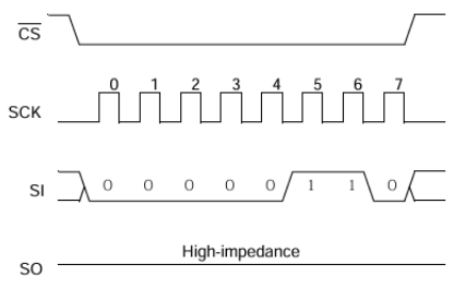
If you do not set the write enable latch (WEL) or toggle the CS line, a silent failure occurs.
2. Initiate a write operation with the WRITE instruction by completing this page write sequence:
Drive CS line low > Send 0x02 (WRITE) > Send 16-bit Address > Send Data (Max 16 bytes) > Drive CS line high after data byte is transferred
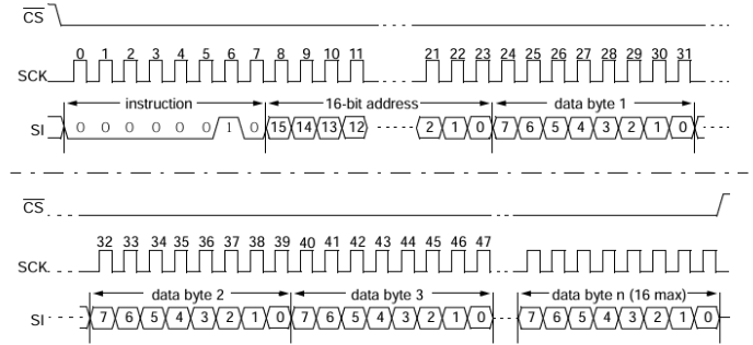
3. Trigger a write cycle.
To write data to memory, drive the CS line high after the least significant bit (D0) of the last data byte has been clocked in. Otherwise, the write operation does not complete.
The Microchip 25XX080 8K SPI Bus Serial EEPROM datasheet mentions that the internal write cycle time (Twc) is a maximum of 5 ms and an attempt to read from a memory location is not possible during a write cycle.
The write enable latch (WEL) is automatically reset when the write cycle is completed.
Read from EEPROM
Initiate a data read from an address of the EEPROM after confirming that data was successfully written. You have two options for checking the status of a write operation:
Wait for a maximum of 5 ms of write cycle time.
Poll the Write-In-Process (WIP) bit in the Read Status Register (RDSR), which is at address 0x05.
To poll the WIP bit:
Drive CS line low → Send
0x05(RDSR) → Send a dummy byte (0x00) to read the 8-bit register value.Check bit 0 (WIP). A value of 1 indicates Busy (the write is in progress). A value of 0, indicates Ready (the write is complete).
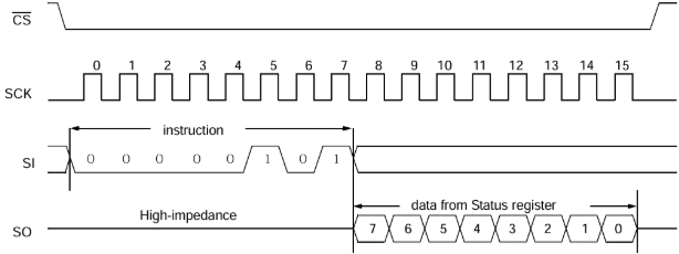
To read from the EEPROM, initiate this sequence of operations:
Drive CS line low.
Send
0x03(READ).Send 16-bit address (MSB then LSB).
Send dummy bytes to clock out data.
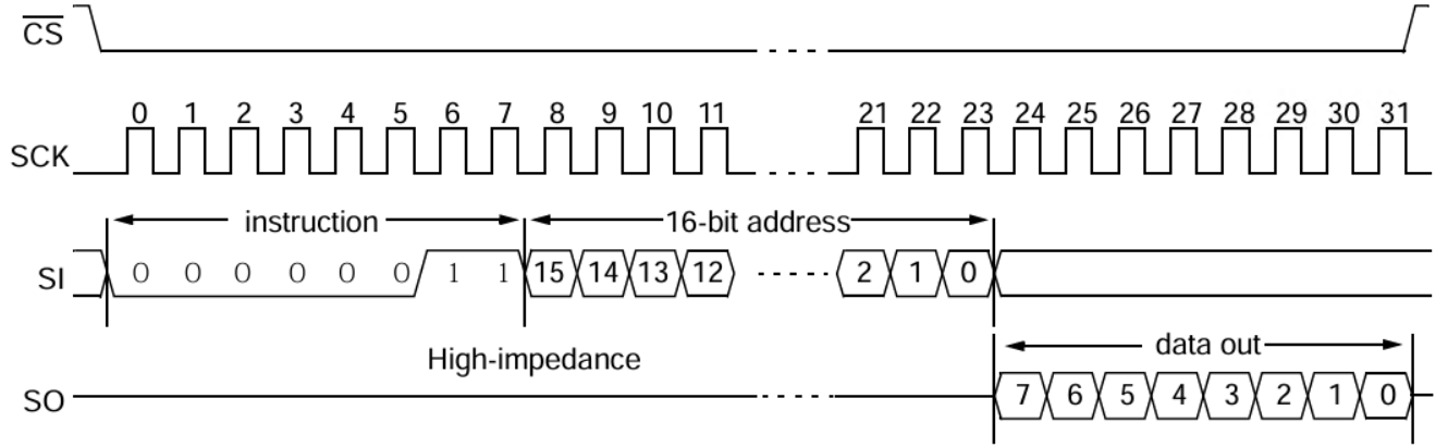
The address pointer automatically increments, allowing the entire array to be read in a single sequence,
Set Up Hardware Connections
Hardware connections depend on whether you use the EEPROM in your application. In this example, the Renesas RH850 board (acting as SPI controller) connects to a 25AA080 SPI EEPROM chip using MSPI0.
25AA080 EEPROM Pin | RH850/U2A16 (MSPI0) |
|---|---|
CS (Pin 1) | P2_3 |
SO (Pin 2) | P6_7 |
/WP (Pin 3) | 3.3 V |
VSS (Pin 4) | GND |
SI (Pin 5) | P6_9 |
SCK (Pin 6) | P6_8 |
HOLD (Pin 7) | 3.3 V |
VCC (Pin 8) | 3.3 V |
Read and Write EEPROM Data Using SPI Controller Transfer Block
Open the RH850spiEEPROM.slx Simulink model.
modelName = "RH850spiEEPROM";
open_system(modelName) 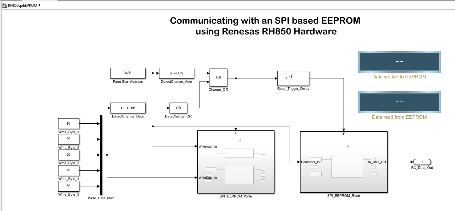
The model is pre-configured for Renesas RH850 U2A Based hardware.
Ensure the following settings are applied:
spi_eeprom_example.arxmlis added as the configuration description file in Build options. To verify click Modeling > Model Settings to open the Configuration Parameters dialog box. Navigate to Hardware Implementation > Target hardware resources > Build options.
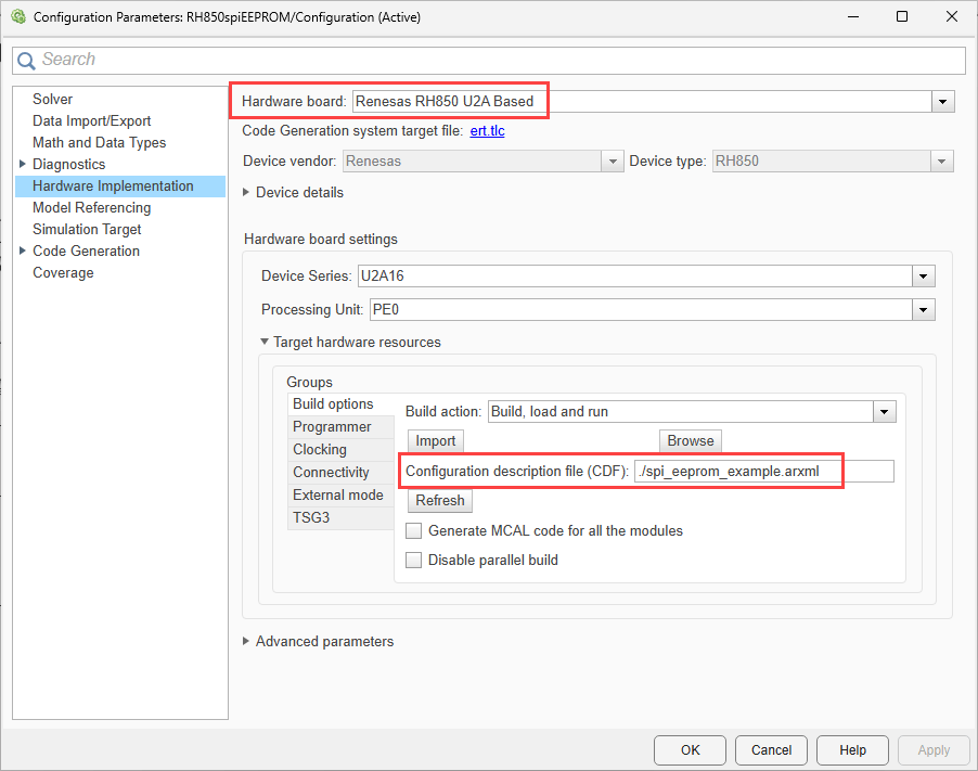
The model contains two main subsystems:
SPI_EEPROM_Write — performs the EEPROM write-enable and page-write operations
SPI_EEPROM_Read — performs the EEPROM read operation
Model Overview
The example model (RH850spiEEPROM) demonstrates both write and read operations with the 25AA080 EEPROM using a single Simulink model. The model uses the MCAL SPI block configured for synchronous transmission.
EEPROM Write Subsystem
This subsystem contains two SPI blocks executed in priority order. WREN must always be Priority 1 because the WEL bit is required by the EEPROM before it will accept a WRITE command.
SPI Transfer Execution Order
Priority | Block | SPI Sequence | Purpose |
|---|---|---|---|
1 | SPI_WriteEnable | SpiWriteEnableSequence | Sends WREN (0x06) command to set the Write Enable Latch (WEL). |
2 | SPI_WriteData | SpiWriteSequence | Sends the WRITE command (0x02), EEPROM address, and data bytes. |
Note: The EEPROM automatically clears the Write Enable Latch (WEL) after each successful write operation. Therefore, the WREN command (0x06) must be sent before every WRITE operation. Sending WREN only during initialization can cause subsequent write operations to be ignored.
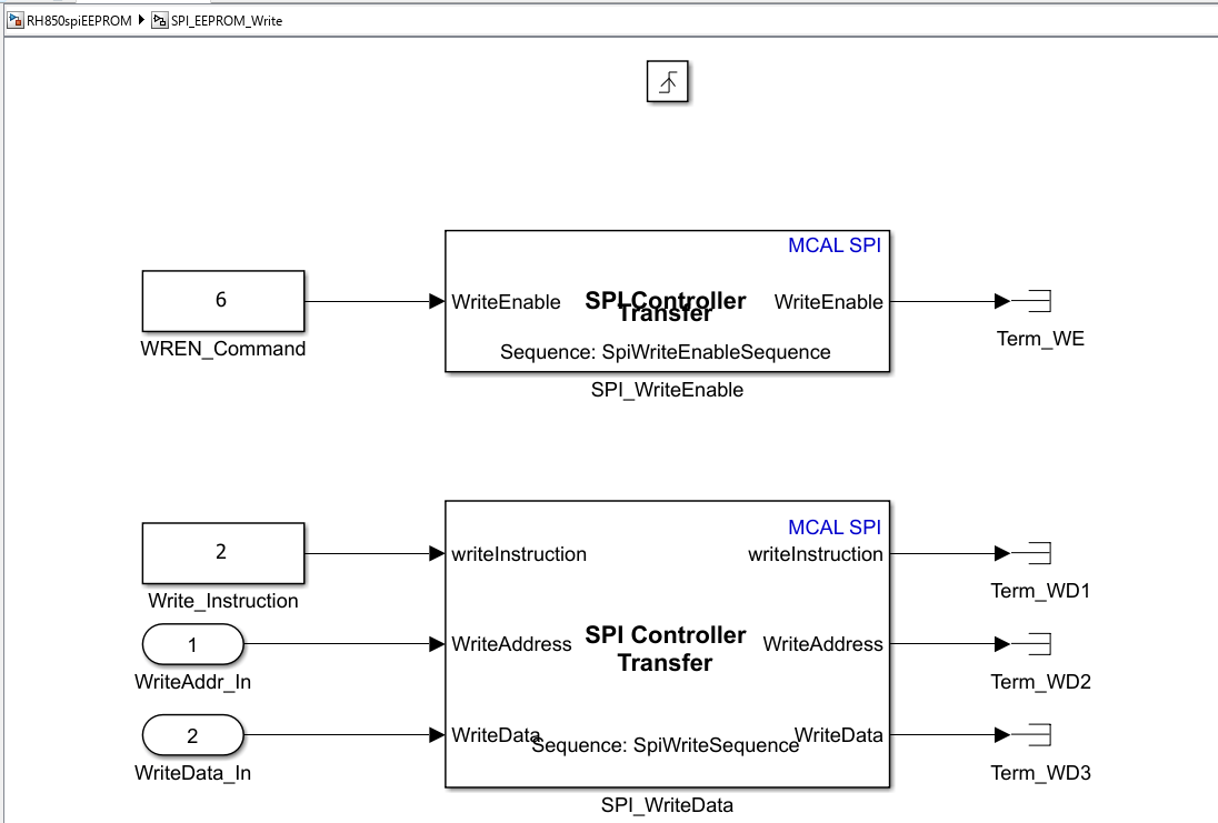
EEPROM Read Subsystem
The SPI EEPROM Read subsystem executes when a change in the write address or write data generates a rising-edge trigger. The subsystem reads data from the EEPROM using the configured SPI read sequence and returns the received data for display and verification.
Priority | Block | SPI Sequence | Purpose |
|---|---|---|---|
1 |
| SpiReadSequence | Sends READ instruction ( |
Received Data Handling
The SPI receive buffer contains both transmitted and received information. The instruction byte and address bytes returned by the EEPROM are discarded, while the received EEPROM data bytes are forwarded to the display block for comparison with the transmitted data.
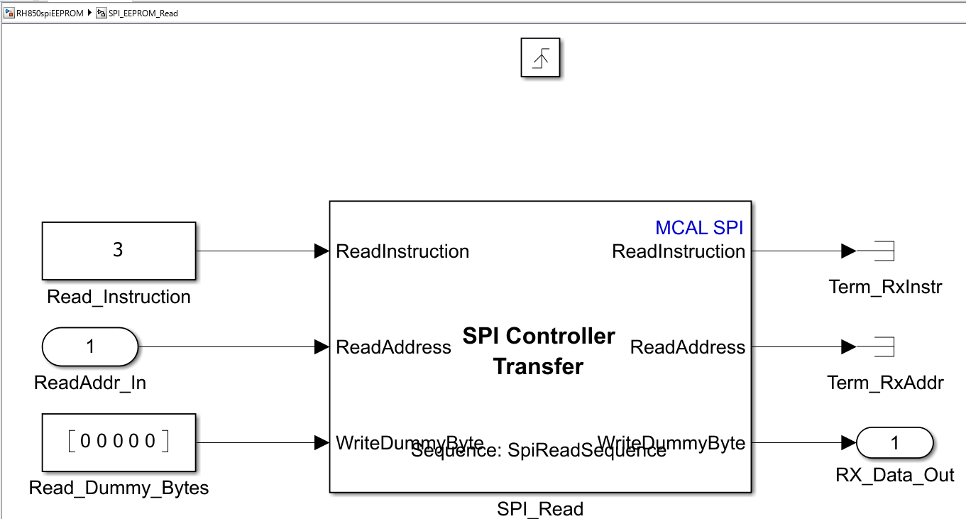
Monitor and Tune the Model on Hardware
In the Simulink model, click Hardware tab and then click Monitor & Tune.This deploys the model to the target hardware.

Observe the displayed values for:
Data written to EEPROM
Data read from EEPROM
If the configuration is correct, the read-back data should match the values written to the EEPROM.
Results
When the model runs:
The write-enable sequence sends the
0x06command.The write sequence sends the
0x02command, the target address, and the write data.The read sequence sends the
0x03command, the read address, and the required dummy bytes.The EEPROM returns the stored data on the SPI receive line.
The model displays the transmitted and received values for comparison.

