Integrated EM and Circuit Co-Simulation of Microstrip Transitions and Device Loading
R2026bThis example demonstrates a practical and structured workflow for combining full-wave electromagnetic (EM) simulation using RF PCB Toolbox™ with circuit-level simulation using RF Toolbox™. The objective is to show how to extract an EM model of a PCB structure, expose an internal port, and then integrate lumped elements or measured S-parameters without repeatedly re-running the EM solver.
The workflow proceeds in a logical sequence. First, build a PCB EM model consisting of microstrip traces over a grounded dielectric substrate. This establishes the distributed electromagnetic behavior of the structure. Next, create a slot gap in the trace and add internal ports across the gap. Then extract the EM model as S-parameters and create a pcbElement object. Finally, calculate the S-parameters of the pcbElement, which now represents the combined EM structure and attached circuit elements. This separation allows the geometry to be solved once while the circuit loading can be modified efficiently.
The steps needed to create this workflow:
Build a PCB EM model (microstrip traces over a ground plane).
Introduce a slot gap and add internal ports at the location where a passive needs to be connected.
Extract the EM model as S-parameters and create
pcbElementcircuit object.Calculate the S-parameters for the
pcbElementwhich includes the EM and the circuit.
Different cases shown in the example are:
Basic Simulation with a single Microstrip line.
A lumped capacitor connected in between the microstrip lines
A resonant loading network (capacitor + shunt inductor) connected in between the microstrip lines
An s-parameter of an amplifier connected in between the microstrip lines
Tapered Microstrip Transition for RFIC Pin Matching Using
traceTapered
Although the geometry here is intentionally simple (two microstrip traces), the same approach extends directly to more complex RF PCBs such as filters, couplers, transitions, feed networks, antenna feeds, and mixed EM/circuit assemblies.
Parameters and Frequency Sweep
clear; clc; close all;
boardL   = 40e-3;   % (m)
boardW   = 40e-3;   % (m)
traceL   = 20e-3;   % (m)
traceW   = 5e-3;    % (m) baseline trace width
gap      = 2e-3;    % (m) slot cut length
f = linspace(0.1e9, 5e9, 101);
warning off;
Case 1: Basic Microstrip Line Creation and Simulation
Construct a simple microstrip transmission line structure and prepare it for full-wave electromagnetic (EM) simulation. This serves as the foundation for the entire workflow. The objective here is to build a clean two-port PCB model, extract its S-parameters, and establish a baseline distributed structure before introducing internal ports or circuit-level co-simulation.The first step defines the horizontal placement of the two microstrip traces. The variables x1 and x2 position the traces symmetrically about the board center, at –10 mm and +10 mm respectively. This creates two independent transmission paths separated in space. While they are not electrically connected to each other, they are both modeled on the same PCB stackup and can be individually excited through their ports.
x1 = -10e-3;        % left trace center x
x2 = +10e-3;        % right trace center x

% Board / ground primitives (reused)
boardShape = traceRectangular("Center",[0 0], "Length",boardL, "Width",boardW);
gnd        = traceRectangular("Center",[0 0], "Length",boardL, "Width",boardW);

pcbA = pcbComponent;

line1A = traceRectangular("Center",[x1, 0], "Length",traceL, "Width",traceW);
line2A = traceRectangular("Center",[x2, 0], "Length",traceL, "Width",traceW);
TopA   = line1A + line2A;

pcbA.BoardShape = boardShape;
pcbA.Layers     = {TopA, pcbA.Substrate, gnd};

pcbA.FeedFormat    = "FeedLocations";
pcbA.FeedLocations = [(-traceL/2 + x1)  0  1  3;    % Port 1 (external)
    ( traceL/2 + x2)  0  1  3];   % Port 2 (external)

figure('Name','Geometry - Case 1 (2-port)');
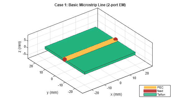
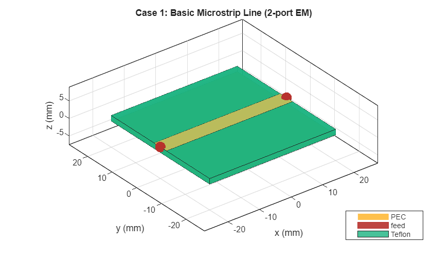
show(pcbA); title("Case 1: Basic Microstrip Line (2-port EM)");
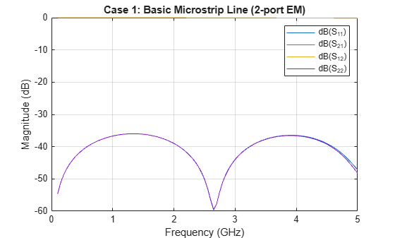
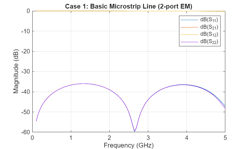
Plot the S-Parameters of the Microstrip Line using the sparameters method.
spar1 = sparameters(pcbA, f, 50,'Sweep','Interp');
figure('Name','S-Parameters - Case 1 (2-port EM)');
rfplot(spar1);
title("Case 1: Basic Microstrip Line (2-port EM)");
Case 2 : Create an Internal EM Interface (4-Port) by adding a Slot Gap and connect a lumped capacitor in the slot
In this case Subtract a narrow rectangular “slot” region from the top metal at the center. Then we add two more feeds at the slot edges to create a 4-port EM structure:
Ports 1–2: external line ends (main signal path)
Ports 3–4: internal ports at the gap edges (to attach components in circuit co-sim)
Begin by creating a new pcbComponent object. Recreate the two rectangular microstrip traces using traceRectangular, and position them symmetrically about the board center using the previously defined x1 and x2 values. Combine the two traces using the + operator to form the top metal layer. At this stage, the geometry matches the baseline structure from Case 1.
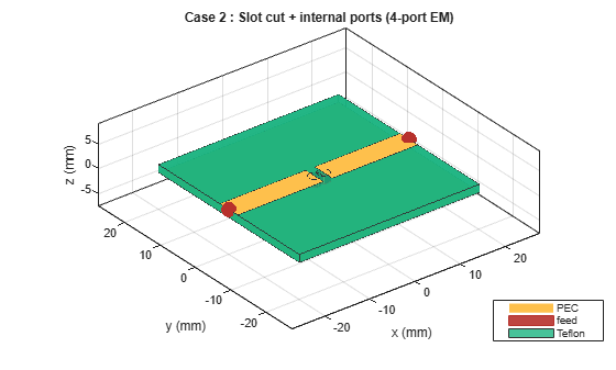
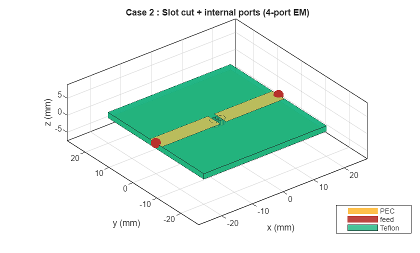
Next, create a slot in the top conductor to expose an internal port. Use traceRectangular to define a narrow rectangular shape centered at the origin. This rectangle represents the physical gap in the microstrip. Subtract this shape from the combined top layer using the - operator. This operation removes metal in the center region and creates a discontinuity. Physically, this forms a gap in the trace. Electrically, this gap defines a controlled location where a circuit element or measured network can later be inserted.
pcbB = pcbComponent;

line1B = traceRectangular("Center",[x1, 0], "Length",traceL, "Width",traceW);
line2B = traceRectangular("Center",[x2, 0], "Length",traceL, "Width",traceW);
TopB   = line1B + line2B;

% Slot cut in top conductor (reused later)
gapCut = traceRectangular("Center",[0 0], "Length",gap, "Width",boardW);
TopB   = TopB - gapCut;

pcbB.BoardShape = boardShape;
pcbB.Layers     = {TopB, pcbB.Substrate, gnd};

pcbB.FeedFormat = "FeedLocations";
pcbB.FeedLocations = [(-traceL/2 + x1)  0  1  3;    % Port 1 (external)
    ( traceL/2 + x2)  0  1  3;    % Port 2 (external)
    (-gap/2)          0  1  3;    % Port 3 (internal, left slot edge)
    ( gap/2)          0  1  3];   % Port 4 (internal, right slot edge)
Use the show function to visualize the geometry. Carefully inspect the plot to confirm that the slot appears correctly and that all four ports are positioned as intended. Verifying the geometry at this stage helps prevent incorrect port assignments or unintended metal connections.
figure('Name','Geometry - Case 2 (4-port interface)');
show(pcbB); title("Case 2 : Slot cut + internal ports (4-port EM)");
Use the sparameters function to compute the full-wave EM response of the four-port structure. Provide the frequency vector f and set the reference impedance to 50 ohms. Use the 'Sweep','Interp' option to enable interpolated frequency sweeping, which improves simulation speed by solving at selected frequency points and interpolating intermediate results.The function returns a four-port S-parameter object. This object contains complete network information, including reflections at all ports and transmission between every port pair. Unlike the two-port case, this model now captures the electrical behavior across the slot interface and the coupling between external and internal ports.
sparB4 = sparameters(pcbB, f, 50,'Sweep','Interp');
figure('Name','S-Parameters - Case 2 (4-port EM)');
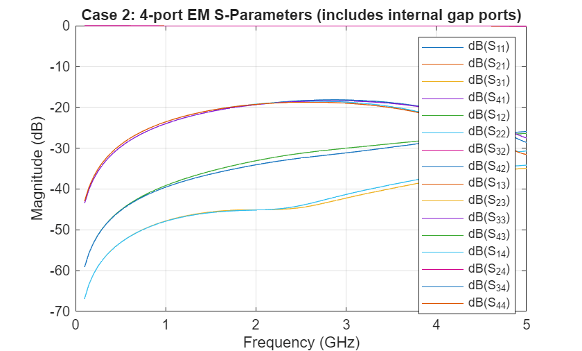
Use the rfplot function to plot the S-parameters. Examine the reflection and transmission responses to understand how the slot affects signal propagation. This four-port EM model now serves as a reusable building block. Ports 1 and 2 define the external RF Ports, while Ports 3 and 4 define an internal port. In the next step, use these internal ports to connect lumped elements or measured network blocks in a circuit-level co-simulation without modifying or re-solving the EM geometry
rfplot(sparB4);
title("Case 2: 4-port EM S-Parameters (includes internal gap ports)");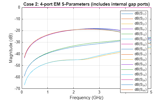
Use the pcbElement function to convert the PCB geometry into a circuit-compatible element. This object allows you to attach lumped components directly across specified ports of the EM structure. It acts as a bridge between full-wave EM modeling and circuit-level loading. Use the PortNumber property to specify the pair of ports across which the lumped element will be connected. In this case, connect the component between Port 3 and Port 4. These are the internal ports located on either side of the slot. By doing this, you effectively bridge the gap with the capacitor. Use the PortValue property to assign the component that will be connected across the specified port pair. Use the capacitor to create a lumped capacitor object with the value Cgap. This operation inserts the capacitor directly across the slot inside the EM structure. Use the AnalysisPorts property to specify which ports define the system-level input and output. In this case, analyze the network as a two-port system between Port 1 and Port 2. The internal ports (3 and 4) remain internal ports and are no longer treated as external measurement ports.
Cgap = 5e-11;  % Farads
ckt2 = pcbElement(pcbB);
ckt2.PortNumber={{3,4}};
ckt2.PortValue = {capacitor(Cgap)};
ckt2.AnalysisPorts = {1,2};
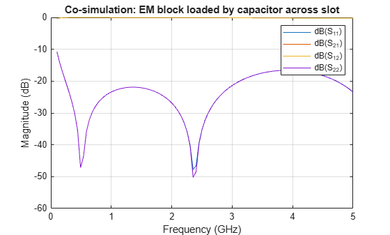
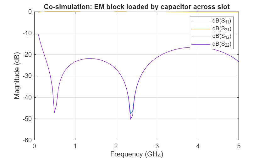
Use the sparameters function to calculate the frequency response of the EM structure with the capacitor included. This step performs the co-simulation. The EM solver behavior is preserved, but the slot discontinuity is now electrically bridged by the lumped capacitor. Use the rfplot function to plot the S-parameters of the loaded structure. Observe how the capacitor modifies the transmission and reflection behavior compared to the open-slot case. Depending on the capacitance value, you may see resonance behavior, impedance transformation, or improved coupling across the gap.
spar2 = sparameters(ckt2, f);
figure('Name','Co-sim - EM + Capacitor');
rfplot(spar2);
title("Co-simulation: EM block loaded by capacitor across slot");
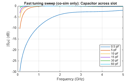
Fast Tuning Sweep: Change capacitor value without re-solving EM
In this section, perform a fast tuning sweep by varying the capacitor value connected across the internal slot. Use this approach to study how different capacitance values affect the transmission response without modifying the PCB geometry or re-creating the EM model. Use the sparameters function to compute the network response of the loaded structure for the current capacitance value. This step performs circuit-level co-simulation using the already-solved RF PCB. Inside the loop, update the capacitor value connected across Ports 3 and 4 by modifying the PortValue property of ckt2. Use the sparameters function to compute the network response of the loaded structure for the current capacitance value.
Cvec = [0.5 5 10 15 30 60]*1e-12;
S21magTune = zeros(numel(f), numel(Cvec));

for k = 1:numel(Cvec)
    ckt2.PortValue = {capacitor(Cvec(k))};
    spTune = sparameters(ckt2, f);
    S21_1 = rfparam(spTune,2,1);
    S21magTune(:,k) = 20*log10(abs(S21_1));
end
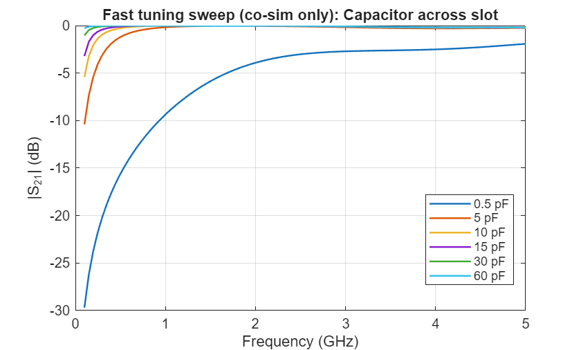
Use the plot function to display all transmission curves on the same figure. Observe how increasing the capacitance changes the transmission behavior. Larger capacitance values will exhibit smaller reactance at high frequency and will behave as a short circuit, thereby reducing the Insertion Loss.
figure('Name','Tuning Sweep - Capacitor Across Slot');
plot(f/1e9, S21magTune, 'LineWidth', 1.2);
grid on;
xlabel("Frequency (GHz)");
ylabel("|S_{21}| (dB)")
legend("0.5 pF","5 pF","10 pF","15 pF","30 pF","60 pF","Location","best");
title("Fast tuning sweep (co-sim only): Capacitor across slot");
Case 3: Resonant Loading: Capacitor + Shunt Inductor to Ground
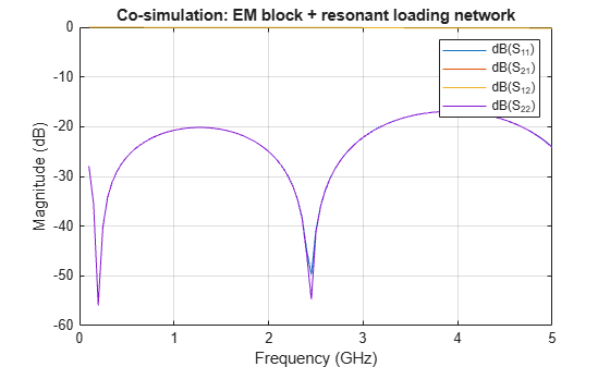
Define a resonant network and attach it to the internal port to study how a local resonator loads the PCB. Use this pattern to model traps, tuned loading, or an IC input that has both capacitive and inductive parasitics. Use PortValue to provide the actual lumped elements in the same order. Here the capacitor Cgap bridges the gap and identical inductors Lsh are placed as shunt elements on each side of the slot. Use AnalysisPorts to tell the solver to treat ports 1 and 2 as the external two-port that you want to analyze; ports 3 and 4 are internal ports.
Lsh = 1e-2;  % Henries (illustrative)
Cgap = 3e-10;  % Farads
ckt3 = pcbElement(pcbB);
ckt3.PortNumber={{3,4},{3,0},{4,0}};
ckt3.PortValue = {capacitor(Cgap),inductor(Lsh),inductor(Lsh)};
ckt3.AnalysisPorts = {1,2};

spar3 = sparameters(ckt3, f);

figure('Name','Co-sim - Resonant Load');
rfplot(spar3);
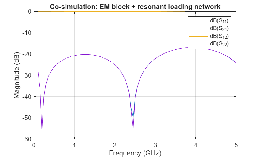
title("Co-simulation: EM block + resonant loading network");
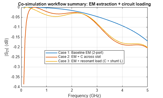
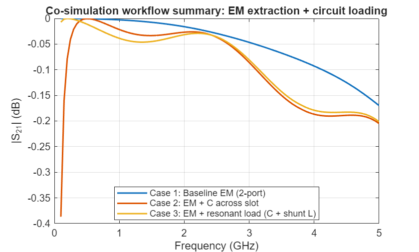
Results Summary: Overlay |S21| (dB) for all the three use cases.
In this section, compare the transmission behavior of the different configurations to understand how circuit loading modifies the EM response. Focus on the magnitude of S21, which represents forward transmission through the structure.
spar1corresponds to the baseline two-port EM model (no slot loading).spar2corresponds to the EM model loaded with a capacitor across the slot.spar3corresponds to the EM model loaded with the resonant network (capacitor + shunt inductors).
Use the plot function to display all three transmission curves on the same axes. Use hold on to overlay multiple curves on a single figure. Add grid lines and axis labels for clarity.
Use the legend function to clearly identify each configuration. This makes it easy to see how the baseline EM structure compares to the capacitor-loaded and resonator-loaded cases. Finally, use the title function to describe the purpose of the plot.
S21 = rfparam(spar1, 2, 1);
S21A = 20*log10(abs(S21));

S21 = rfparam(spar2, 2, 1);
S21C = 20*log10(abs(S21));

S21 = rfparam(spar3, 2, 1);
S21D = 20*log10(abs(S21));

figure('Name','Comparison - |S21| Overlay');
plot(f/1e9, S21A, 'LineWidth', 1.5); hold on;
plot(f/1e9, S21C, 'LineWidth', 1.5);
plot(f/1e9, S21D, 'LineWidth', 1.5);
grid on;
xlabel("Frequency (GHz)");
ylabel("|S_{21}| (dB)");
legend("Case 1: Baseline EM (2-port)", ...
    "Case 2: EM + C across slot", ...
    "Case 3: EM + resonant load (C + shunt L)", ...
    "Location","best");
title("Co-simulation workflow summary: EM extraction + circuit loading");
Case 4 : An s-parameter of an Amplifier connected in between the microstrip lines
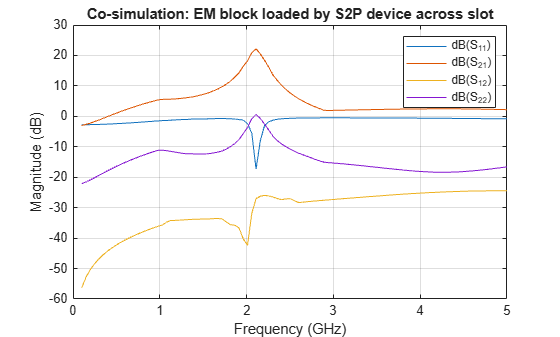
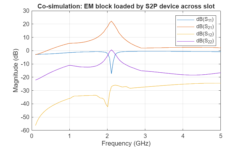
Replace the lumped element with a measured or vendor two-port Touchstone file so that the EM simulation result is connected with a real device model (for example, an amplifier, filter, or connector). This lets you evaluate the combined EM + device behavior using the measured frequency-dependent network rather than an idealized lumped component. Use a valid two-port Touchstone file on your MATLAB path (or provide the full path). The pcbElement object reads the file and inserts the measured network across the specified internal ports. Use sparameters with the frequency vector f to evaluate the frequency-dependent response of the entire assembly (EM simulation result + Touchstone device). Ensure that the Touchstone file uses the same reference impedance (typically 50 Ω) as your EM simulation; if not, perform de-embedding or impedance conversion as needed.
s2pFile = 'default.s2p';
ckt4 = pcbElement(pcbB);
ckt4.PortNumber={{3,4}};
ckt4.PortValue = {s2pFile};
ckt4.AnalysisPorts = {1,2};
spar4 = sparameters(ckt4, f);
figure('Name','Co-sim - EM + S2P Device');
rfplot(spar4);
title("Co-simulation: EM block loaded by S2P device across slot");
Case 5 : Tapered Microstrip Transition for RFIC Pin Matching Using traceTapered
The width of the IC pin is taken as 2 mm and the input line width is taken as 5 mm which corresponds to 50 ohm for the Teflon substrate of height 1.6 mm. Define the tapered transition geometry. Use traceTapered to create a taper that transitions the wide 5 mm input trace to the narrow 2 mm IC pin. In this example Shape1 creates a two-stage taper (first segment 8 mm, second 4 mm) anchored so the left taper sits around -7 mm on the x-axis. The vector for Length implements a multi-segment taper so you can control the taper profile more flexibly than with a single straight segment.
Create the symmetric counterpart for the other side. Use mirrorY to produce Shape2 as the mirror image about the y-axis and then combine them. This yields two opposing tapered traces that meet at the board center where the IC pin lands. Use show(pcb) later to visually confirm the smooth geometry and the matching pin land widths.
Shape1 = traceTapered("InputWidth",5e-3,"OutputWidth",2e-3,"Length",[8e-3 4e-3],"ReferencePoint",[-7e-3,0]);
Shape2 = mirrorY(copy(Shape1));
warning off;
topLayer = Shape1+Shape2;
gndLayer = traceRectangular("Length",26e-3,"Width",20e-3);
substrate = dielectric("Teflon");
pcb = pcbComponent;
pcb.BoardShape = gndLayer;
pcb.Layers = {topLayer,substrate,gndLayer};

pcb.FeedLocations = [-13e-3 0 1 3;13e-3 0 1 3;-1e-3 0 1 3;1e-3 0 1 3];
pcb.FeedDiameter = [2.5e-3 2.5e-3 1e-3 1e-3];
figure,show(pcb);
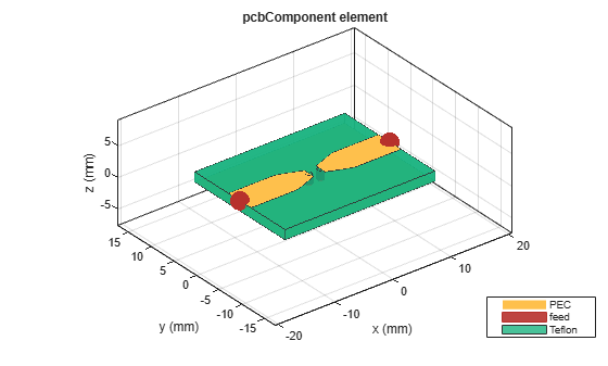
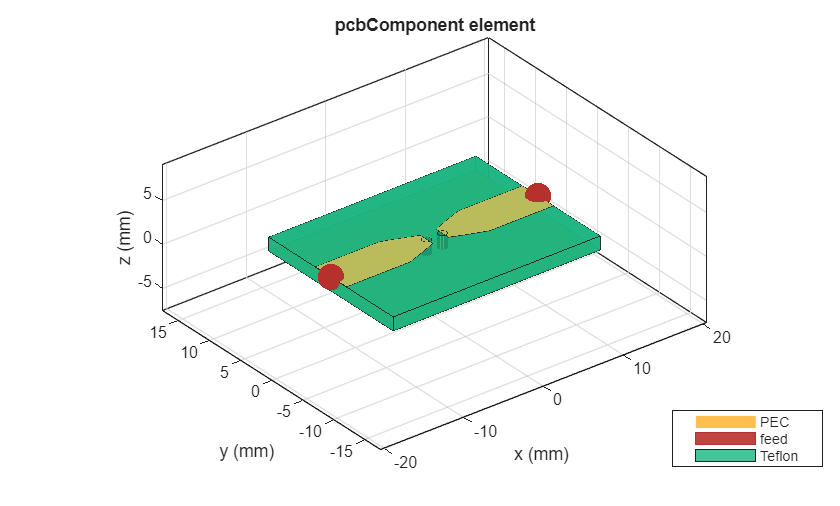
Run EM simulation to get the S-parameters for the tapered geometry. Use sparameters to compute the full-wave response over the frequency vector f. Inspect the structure with show(pcb) before EM Simulation and use the plotted S-parameters to validate expected propagation, impedance continuity through the taper, and any unexpected reflections from the transition.
spar = sparameters(pcb,f);
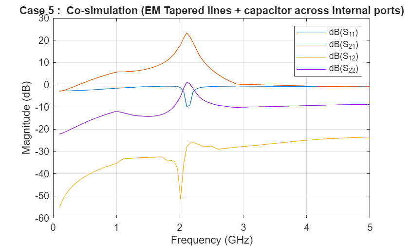
Attach an amplifier across the internal port using the pcbElement object. Use pcbElement and the properties PortNumber, PortValue, AnalysisPorts to connect an s2p file between the two internal ports and to treat Ports 1 and 2 as the external analysis ports. Then use sparameters to compute the loaded response without re-computing the EM geometry. This reuses the expensive EM simulation and lets you evaluate the s-parameters along with the amplifier s2p file.
cktC = pcbElement(pcb);
cktC.PortNumber={{3,4}};
cktC.PortValue = {s2pFile};
cktC.AnalysisPorts = {1,2};

spar5 = sparameters(cktC, f);

figure('Name',"Case 6 Co-sim (EM Tapered Lines + C)");
rfplot(spar5);
title("Case 5 :  Co-simulation (EM Tapered lines + capacitor across internal ports)");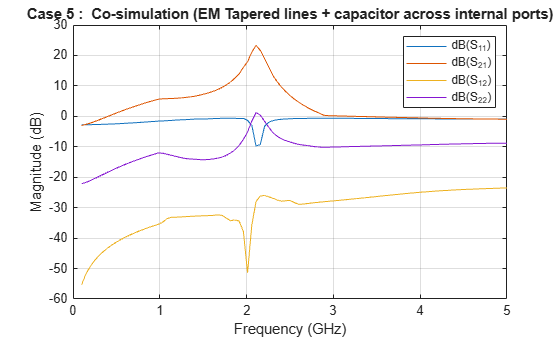
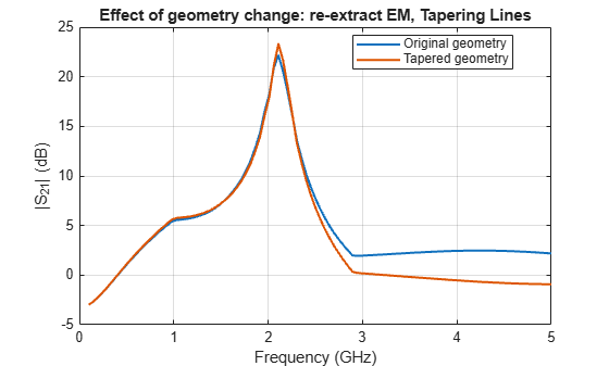
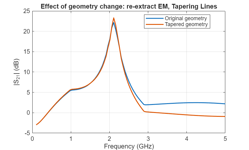
Extract the transmission magnitudes for the original and modified geometries. Plot both curves on the same frequency axis using plot to show how the geometry change affects |S21|. Use the overlay to observe shifts in insertion loss, resonant peaks/notches, and any frequency-dependent phase or magnitude differences introduced by the tapered trace.
% Compare |S21| on a common frequency axis by interpolating the original case
S21 = rfparam(spar4, 2, 1);
S21E = 20*log10(abs(S21));

S21 = rfparam(spar5, 2, 1);
S21F = 20*log10(abs(S21));

figure('Name','Width Change Impact - |S21|');
plot(f/1e9, S21E, 'LineWidth', 1.5); hold on;
plot(f/1e9, S21F, 'LineWidth', 1.5);
grid on;
xlabel("Frequency (GHz)");
ylabel("|S_{21}| (dB)");
legend("Original geometry", ...
    "Tapered geometry", ...
    "Location","best");
title("Effect of geometry change: re-extract EM, Tapering Lines");