Microstrip Band-pass filter based RF Filter Bank for microwave applications
RF Filter banks are used in many applications such as wide-band receivers that detect signals over a wide frequency band. This example shows how to create an RF filter bank using pcbcascade functionality and analyze it using a full wave solver. The filters used in the RF filter bank have been created and optimized in the other examples and the filter objects and sparameters from those examples are imported into this example from a MAT file.
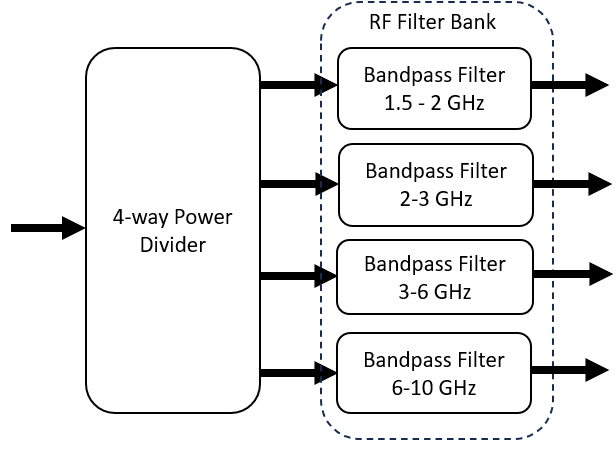
The filters mentioned above are designed and analyzed using full wave MoM solver and optimization using patternSearch and sorrogateOpt methods from Global Optimization toolbox are used to optimize for more bandwidth and better S11 and S21. The below table lists out the filters and the technique used to design these filters.
Filter Type | Filter Geometry | Analysis/Optimization Technique |
Band Pass Filter (1.5 - 2 GHz) | Hairpin Filter | Optimization using Pattern Search |
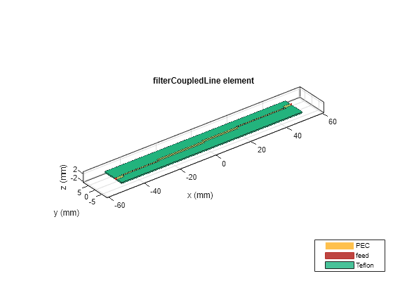
Band Pass Filter (2 - 3 GHz) | Coupled Line Filter | Optimization Using Surrogate Opt |
Band Pass Filter (3 - 6 GHz) | Stub and Stepped Impedance Low Pass | Combining Low Pass and High Pass Filter |
Band Pass Filter (6 - 10 GHz) | Custom Design | Custom geometry creation |
Load the filter data using the load function. The filter data is available in AllFilters.mat. Visualize all the filters using the show method.
load('allDataFilters.mat');
filt1.GroundPlaneWidth = 40e-3;
figure,show(filt_1);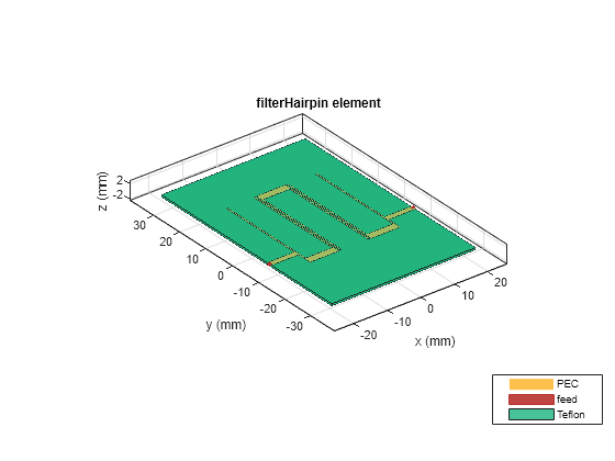
figure,show(filt_2);
figure,show(filt_3);
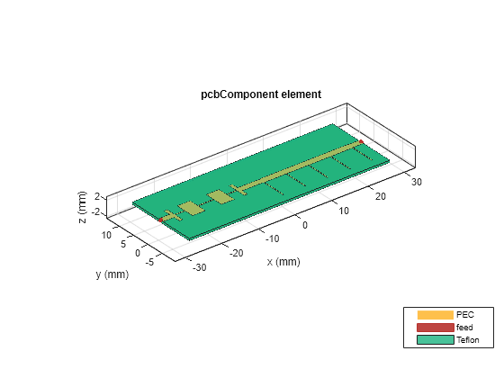
figure,show(filt_4);

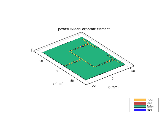
A Power divider is used to divide the signal into four ports to which the filters are connected. Use the powerDividerCorporate object and the Splitter as a wilkinsonSplitterWideband object.
pdc = powerDividerCorporate;
splitter = wilkinsonSplitterWideband;
splitter.Height = 0.508e-3;
pdc.SplitterElement = splitter;
Use the design function to design the powerdividerCorporate at 5 GHz and set the desired PortSpacing for the output ports and visualize the geometry.
pdc = design(pdc,5.5e9);
pdc.PortLineWidth = 1.6e-3;
pdc.PortSpacing = 40e-3;
pdc.GroundPlaneWidth = 140e-3;
pdc.MiterDiagonal = 0.5e-3;
figure,show(pdc)
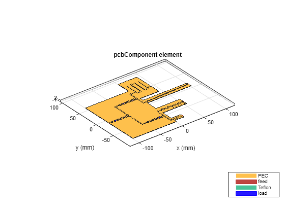
Use the pcbcascade functionality to cascade the second port on the powerDividerCorporate to the first port of the First Filter. Repeat this step to create the cascade of the three other filters and visualize the geometry using the show function. The pcbcascade also opens a GUI when Interactive is set to true. This GUI allows the user to Interactively select the ports on the two objects to be cascaded.
filterBank  = pcbcascade(pdc,filt_1,2,1,"RectangularBoard",false);
filterBank  = pcbcascade(filterBank,filt_2,2,1,"RectangularBoard",false);
filterBank  = pcbcascade(filterBank,filt_3,2,1,"RectangularBoard",false);
filterBank  = pcbcascade(filterBank,filt_4,2,1,"RectangularBoard",false);
figure,show(filterBank);
Use the mesh function to manually mesh the structure by setting the MaxEdgeLength to 6e-3;
figure,mesh(filterBank,'MaxEdgeLength',6e-3);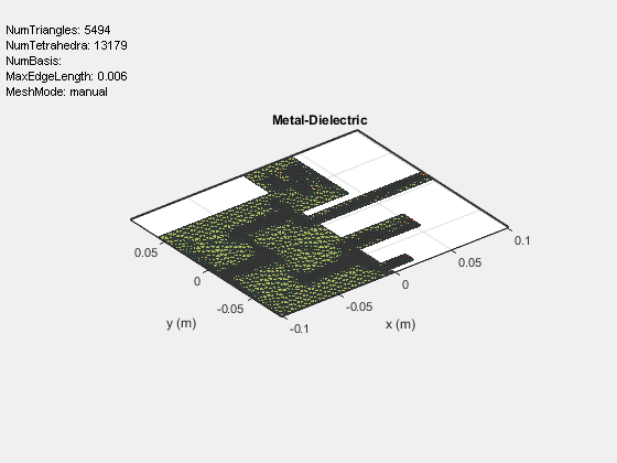
Use the sparameters function to calculate the sparameters of the filter-bank and plot them using the rfplot function. To run the sparameters using a full wave MoM solver, uncomment the below code.
% sparfilterbank1 = sparameters(filterBank,linspace(1e9,12e9,301));
% figure,rfplot(sparfilterbank1,2:5,1);
As this structure is electrically large, it takes a lot of time to compute the sparameters. Hence we use a faster approach to calculate the sparameters of this layout.
Use the mesh function to manually mesh the corporate power divider.
figure,mesh(pdc,'MaxEdgeLength',30e-3);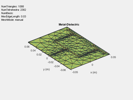
Use the sparameters function to calculate the s-parameters for the corporate power divider and visualize using rfplot function.
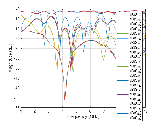
sparpdc = sparameters(pdc,linspace(1e9,10e9,101));
figure,rfplot(sparpdc)
Use the nport object to create the objects for corporate power divider and all the filters, using their respective s-parameters.
ob1 = nport(sparpdc);
ob2 = nport(spar1);
ob3 = nport(spar2);
ob4 = nport(spar3);
ob5 = nport(spar4);
Use the circuit to create a circuit of the n-port objects. Use the add method to add the nport objects for all the filters and assign the ports accordingly. Assign the ports using setports function.
ckt = circuit('FilterBankBeh');
add(ckt,[1 2 3 4 5],clone(ob1))
add(ckt,[2 6],clone(ob2))
add(ckt,[3 7],clone(ob3))
add(ckt,[4 8],clone(ob4))
add(ckt,[5 9],clone(ob5))

setports(ckt,[1 0],[6 0],[7 0],[8 0],[9 0]);
Use the sparameters to compute the s-parameters of the circuit and plot it using the rfplot.
sparbeh = sparameters(ckt,linspace(1e9,14e9,1001));
figure,rfplot(sparbeh,2:5,1);

Using the above shown workflow, any number of RF Filter channels can be realized and layout can be created using pcbcascade functionality. RF Filters can be designed, analyzed using a full wave MoM solver and then combined to created RF Filter Banks.