Design and Analyze Band Stop Filter Using pcbComponent
This example shows you how to design and analyze band stop filter using the pcbComponent object. Design the band stop filter with a fractional bandwidth (FBW) of 1.0 at a midband frequency of 2.5 GHz for the band-edge frequencies of = 1.25 GHz and = 3.75 GHz as defined in Figure 6.11b of reference [1].
Design Band Stop Filter
Design the microstrip band stop filter based on a three-pole (n = 3) Chebyshev lowpass prototype with 0.05 dB passband ripple. The element values of the lowpass prototype are
= = 1.0
= = 0.8794
= 1.1132
Using the design equations Eq.(6.30) given in reference [1] on page no. 182 for n = 3 and = 50 Ω as , you can obtain
= = 50 ohm
= = 106.8544 ohm
= = 93.9712 ohm
= 44.9169 ohm
Choose a commercial substrate (RT/D 6006) with a relative dielectric constant of 6.15 and thickness of 1.27 mm. Calculate the microstrip widths using the microstrip design equations given in Chapter 4 of reference [1]. The figure shows the schematic diagram of the microstrip band stop filter [1] representing various feature dimensions.
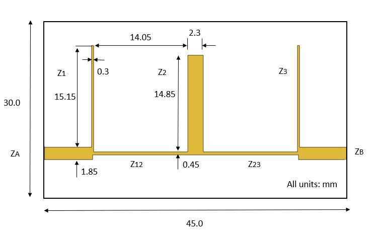
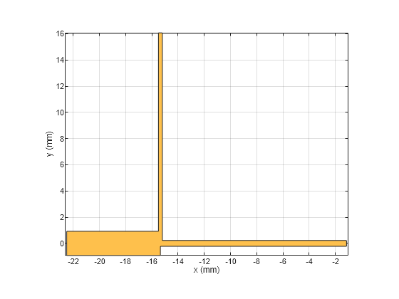
Use the traceRectangular object to create ZA, Z1, Z12. Perform a Boolean add operation for the microstrip shapes ZA, Z1, Z12 and create a LeftSection object. Visualize the LeftSection using show function.
ZA_Width = 1.85e-3;
ZA_Length = 7e-3;
Z1_Length = 0.3e-3;
Z1_Width = 15.15e-3;
Z12_Length = 14.05e-3;
Z12_Width = 0.45e-3;
Z2_Length = 2.3e-3;
Z2_Width = 14.85e-3;
gndL = 45e-3;
gndW = 30e-3;

ZA = traceRectangular(Length = ZA_Length+Z1_Length/2,Width = ZA_Width,...
    Center = [-gndL/2+ZA_Length/2+Z1_Length/4 0]);
Z1 = traceRectangular(Length = Z1_Length,Width = Z1_Width+ZA_Width/2,...
    Center = [-gndL/2+ZA_Length+Z1_Length/2 (Z1_Width/2+ZA_Width/4)]);
Z12 = traceRectangular(Length = Z12_Length+Z1_Length,Width = Z12_Width,...
    Center = [-gndL/2+ZA_Length+Z1_Length/2+Z12_Length/2 0]);
LeftSection = ZA+Z1+Z12;
figure;
show(LeftSection);
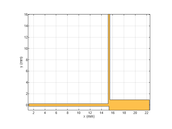
Use the copy, rotateZ and rotateX functions on LeftSection object to create a RightSection. Visualize the RightSection object.
RightSection = copy(LeftSection);
RightSection = rotateZ(RightSection,180);
RightSection = rotateX(RightSection,180);
figure;
show(RightSection);
Perform a Boolean add operation for the shapes LeftSection and RightSection to create a combineSection object. Use the traceRectangular object to create centerArm Z2. Perform a Boolean add operation for the shapes combineSection, Z2, and create a filter object. Visualize the filter object.
combineSection = LeftSection + RightSection;
Z2 = traceRectangular(Length = Z2_Length,Width = Z2_Width,...
    Center = [0 -Z12_Width/2+Z2_Width/2]);
filter = combineSection + Z2;
show(filter);
Define the substrate parameters and create a dielectric to use in the pcbComponent of the designed filter. Create a groundplane using the traceRectangular shape.
substrate = dielectric(EpsilonR = 6.15,LossTangent = 0.0027,...
    Name = "custom",Thickness = 1.27e-3);

ground = traceRectangular(Length = gndL,Width = gndW,...
    Center = [0,6e-3]);
Create PCB Filter Using pcbComponent
Use the pcbComponent to create a filter PCB. Assign the dielectric and ground plane to the Layers property of the pcbComponent. Assign the FeedLocations to the edge of the feed ports. Set the BoardThickness to 1.27 mm on the pcbComponent and visualize the filter.
pcb = pcbComponent;
pcb.BoardShape = ground;
pcb.BoardThickness = 1.27e-3;
pcb.Layers ={filter,substrate,ground};
pcb.FeedDiameter = ZA_Width/2;
pcb.FeedLocations = [-gndL/2 0 1 3;gndL/2 0 1 3];
figure;
show(pcb);
Plot and Analyze the S-Parameters
Use the sparameters function to calculate the s-parameters for the band stop filter and plot it using the rfplot function.
spar = sparameters(pcb,linspace(0.1e9,6e9,50));
figure;
rfplot(spar);
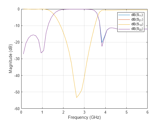
As there are four curves in the result, let us analyze the results.
Analyze the values of , and to understand the behavior of band stop filter.
figure
rfplot(spar,1,1:2)
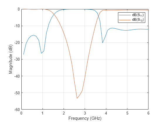
The result shows that the filter has center frequency = 2.5 GHz for the band-edge frequencies = 1.75 GHz and = 3.4 GHz. The values are close to 0 dB and values are less than -10 dB between frequencies = 1.4 GHz and = 3.4 GHz. The designed filter therefore has stopband response. The shift in band-edge frequencies and might be due to use of different full wave numerical solver used for EM simulation.
Visualize Charge and Current Distribution
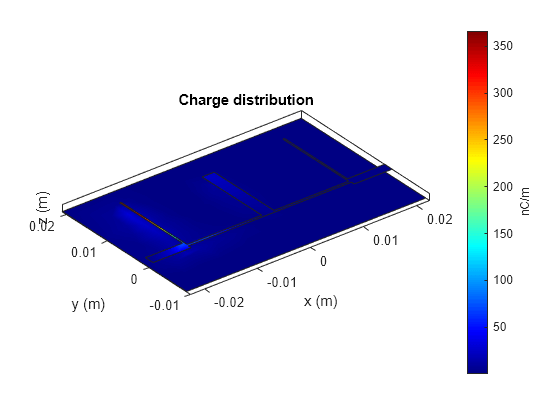
Use the charge function to visualize the charge distribution on the metal surface and dielectric of band stop filter.
figure;
charge(pcb,2.4e9);
figure;
charge(pcb,2.4e9,'dielectric');
Use the current function to visualize the current distribution on the metal surface and the volume polarization currents on dielectric of band stop filter.
figure;
current(pcb,2.4e9);

figure;
current(pcb,2.4e9,'dielectric');
References
[1] Jia-Sheng Hong "Microstrip Filters for RF/Microwave Applications", p. 184, John Wiley & Sons, 2nd Edition, 2011.