Model Clock Recovery Loops in SerDes Toolbox
This example shows how to create detailed models of different types of serial channel clock recovery loops such as Alexander (bang-bang), Meuller-Muller, and Hogg & Chu.
Clock Recovery Model Structure
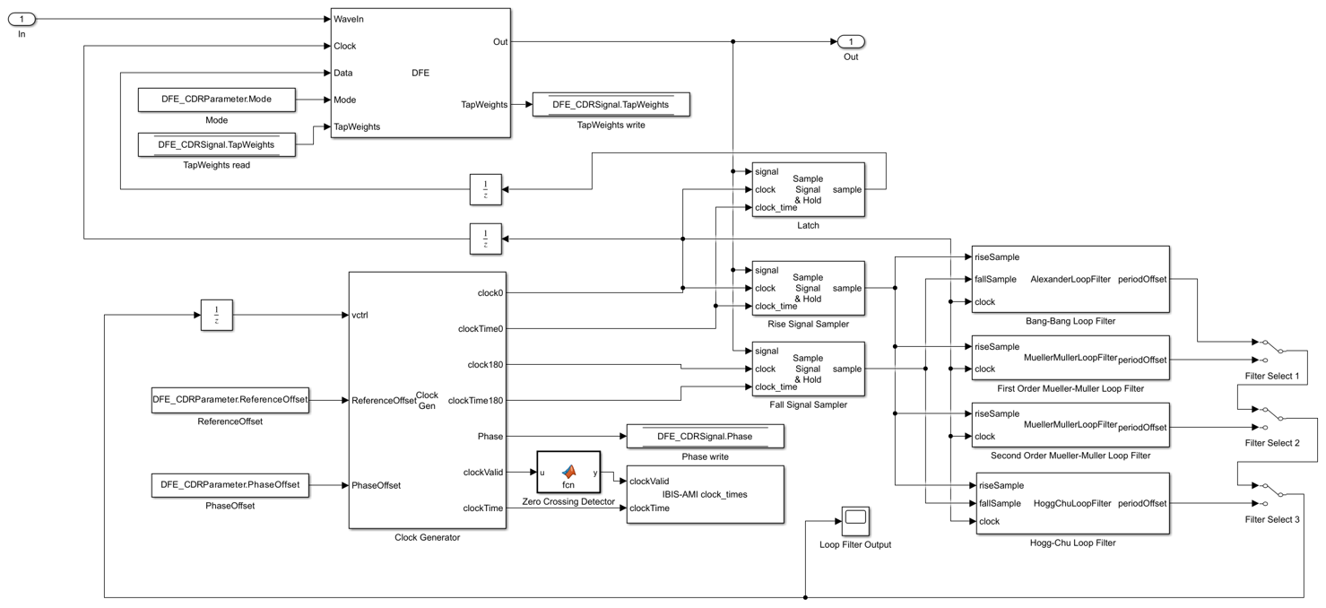
To model a clock recovery loop accurately, the representation of the clock edge times and the associated sampling of the data signal must be as precise as possible. This example demonstrates a method for accomplishing that within a model that uses a fixed step discrete sample time. This method is packaged inside the Clock Generator and Signal Sampler blocks from the Mixed-Signal Blockset™. The Clock Generator models the voltage controlled oscillator (VCO) of the clock recovery loop by maintaining an exact calculation of the clock edge time, including an accurate model of phase noise, and provides the exact clock edge time, along with a saturated clock, to the Signal Sampler. The Signal Sampler models the data decision latch or sample and hold circuit triggered by the clock edge. At the first fixed step sample time after a clock edge, the Signal Sampler applies linear interpolation to its input signal and outputs the resulting estimate of the input signal value at exactly the clock edge time.
The behavior of the clock oscillator and data sampling latch are very similar for different types of clock recovery loops. But the behavior and implementation of the phase detector and loop filter can vary much more widely. For example, for an Alexander clock recovery loop, the phase detection is based on comparison of logic values latched at the rising and falling edges of the clock. In contrast, Hogg & Chu phase detection compares the timing of the clock falling edge with the data threshold crossing time, and Mueller-Muller phase detection depends solely on voltage sampling at the baud rate. The clock recovery loop model treats the loop filter as a separate block, making it as easy as possible to accommodate these differences.
This example also demonstrates the design of a second-order clock recovery loop. The design process is applied to a Mueller-Muller loop filter, but could be applied to the other loop filter types as well.
Example Model Structure
You can develop a model similar to the model in this example by exporting a Simulink® model from the SerDes Designer app. In the receiver model, include a PassThrough block where the clock recovery loop should go, and then manually modify the PassThrough block in Simulink.
To find the clock recovery loop in the model SerdesClockRecovery, open the top level model, then open the receiver block within the example model, and then open the PassThrough block (renamed as DFE_CDR).
open_system('SerdesClockRecovery.slx');
toplevel = gcs;
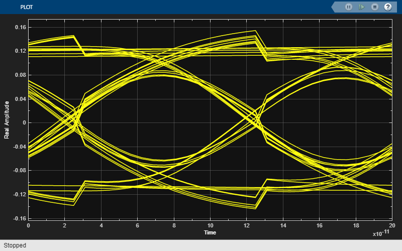
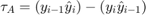
The model exported from the SerDes Designer app consists of a Non-Return to Zero (NRZ) stimulis generator, a transmitter, passive analog channel, receiver and eye diagram display.
Use scope displays to view the data signal and the clock recovery feedback signal.
Open the receiver model to view its internal structure.
open_system('SerdesClockRecovery/Rx');
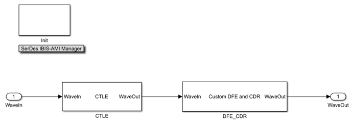
The receiver consists of a Continuous Time Linear Equalizer (CTLE) and a custom block that models the combination of a Decision Feedback Equalizer (DFE) and a Clock/Data Recovery (CDR) block. The CTLE supplies much of the equalization of the received signal, and the DFE adaptively refines the equalization while the CDR adaptively recovers the clock phase.
The DFE and CDR adaptive loops are combined in a single block because the adaptive loops are coupled. Acquisition of the correct clock phase helps the DFE loop configure the optimum equalization, and the DFE equalization helps the CDR loop acquire the correct clock phase.
Open the DFE/CDR block to view its internal structure.
open_system('SerdesClockRecovery/Rx/DFE_CDR','force');
DFE/CDR Model
The DFE is modeled as a single system object that takes the input waveform as an input signal but also requires a recovered clock signal and a signal containing the detected data. The clock is provided by the Clock Generator in the CDR loop while the detected data is provided by a Signal Sampler block ("Latch") connected to the output of the DFE and configured as a latch to model the data decision latch in the receiver. A single sample delay is inserted in both the clock and detected data paths to avoid creating an algebraic loop.
The CDR is modeled using a Clock Generator block to model the VCO in the clock recovery loop and two Signal Sampler blocks ("Rise Signal Sample" and "Fall Signal Sample") to sample the DFE output signal at both the rising and falling clock edges. This configuration reflects typical hardware design practice and does mean, in particular, that the loop filter must output a frequency control voltage rather than a desired phase or similar signal.
The CDR model offers the ability to select between any of four loop filters: Alexander (bang-bang), first order Mueller-Muller, second order Mueller-Muller, and Hogg & Chu. A single sample delay is inserted in the VCO control path to avoid creating an algebraic loop. The loop filters are all implemented as system objects and the example contains the source code for these classes.
The timing in the loop filter is not critical, and loop filter processing can be performed at the sample time when the loop filter receives a clock transition. In particular, the loop filters are coded in a way that does not require knowledge of either the symbol time or the sample interval, thus avoiding problems when generating an IBIS-AMI model through SerDes Toolbox.
Alexander (Bang-Bang) Clock Recovery
The Alexander clock recovery loop detects the clock phase by determining whether the sign of the data signal at the falling edge of the clock matches the sign of the data signal at the rising edge of the clock that occurred either before or after the falling edge. If the sign at the falling edge matches the sign at the previous rising edge but not the subsequent rising edge, then the clock is early. Conversely, if the sign at the falling edge matches the sign at the subsequent rising edge but not the sign at the previous rising edge, then the clock is late. The loop filter is an up-down counter that produces either a positive (early) or negative (late) pulse when it overflows. For a detailed explanation of an Alexander clock recovery loop, see Clock and Data Recovery in SerDes System.
The initial configuration of the SerDesClockRecovery model selects the output of the Alexander loop filter to control the clock phase in the Clocked Sampler.
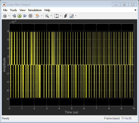
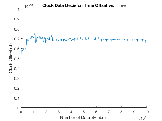
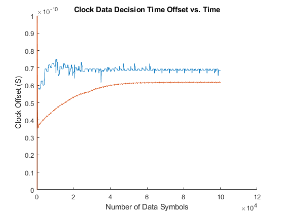
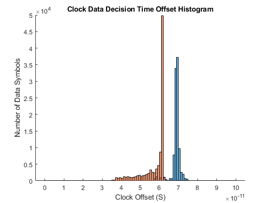
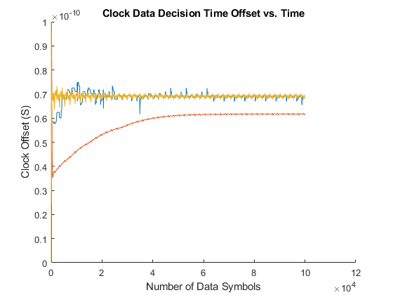
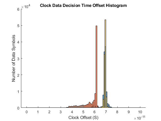
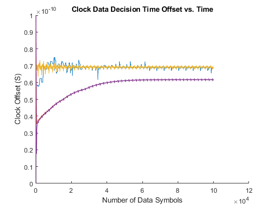
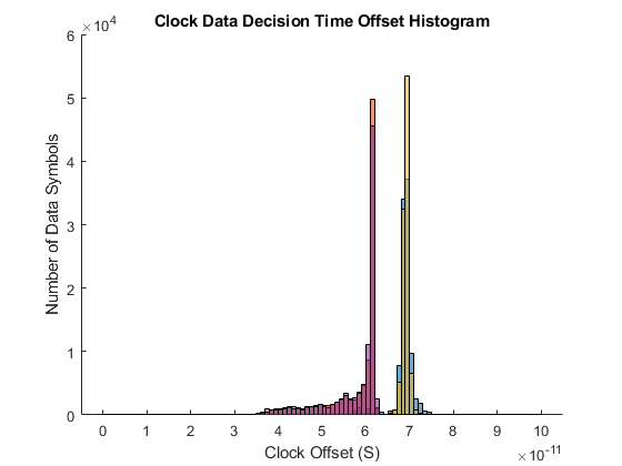
Run the simulation and plot the time history and the histogram of the recovered clock phase. Save the time history of the recovered clock phase to the base workspace so that you can analyze it as you choose.
simout = sim(toplevel);
ctBB = plotClockTimes(simout,toplevel);

Meuller-Muller Clock Recovery
The Meuller-Muller clock recovery algorithm assumes that the data waveform changes fastest when there is a transition between data symbol values, such as a transition from a one to a zero for an NRZ data signal. This assumption enables the clock recovery loop to use one quantitative voltage per symbol, which is an advantage at high data rates. The time error estimate for the example's Meuller-Muller Loop Filter is drawn from CLOCK AND DATA RECOVERY FOR HIGH-SPEED ADC-BASED RECEIVERS, section 2.3.1
where  is the previous voltage sample,
  is the current voltage sample,
  is the previous latched symbol value and
  is the current latched symbol value.
To evaluate the response of the Meuller-Muller clock recovery loop, move the Filter Select 1 switch to its second input port. Run the simulation and add the time history of the recovered clock phase and clock phase histogram to the figures that have already been created for the Alexander clock recovery loop. Save the time history of the clock phase to the base workspace so that you can analyze it later.
set_param([gcs '/Filter Select 1'],'sw','0');
simout = sim(toplevel);
ctMM1 = plotClockTimes(simout,toplevel);

Hogg & Chu Clock Recovery
The Hogg & Chu clock recovery algorithm performs a relatively direct measurement of the clock phase by measuring the time between the threshold crossing of the data signal and the falling edge of the recovered clock. While blocks could be added to the example model to measure the data signal threshold crossing time directly, the Hogg & Chu Loop Filter in this example uses the simplifying approximation that the data signal slope in the threshold crossing region is constant. As estimated once a threshold crossing has been confirmed by the sample at the next clock edge, the time error is

where is the previously detected data symbol value,  is the voltage recorded on the previous clock edge, and
  is the maximum data signal amplitude.
To evaluate the response of the Hogg & Chu clock recovery loop, move the Fiter Select 3 switch to its second input port. Run the simulation, and add the time history of the recovered clock phase and clock phase histogram to the figures that have already been created for the Alexander and Meuller-Muller clock recovery loops. Save the time history of the clock phase to the base workspace so that you can analyze it later.
set_param([gcs '/Filter Select 3'],'sw','0');
simout = sim(toplevel);
ctHC = plotClockTimes(simout,toplevel);

Second Order Clock Recovery
A CDR loop is a phase-locked loop (PLL) for which the clock reference is provided by a received data signal and the phase detector is designed to work with this form of reference. As such, most early CDR loops were first order PLLs; however second order CDR loops are now common. A first order PLL/CDR control loop attempts to minimize the phase error directly while in a second order PLL/CDR control loop includes an integrator that zeros out the frequency offset directly.
The design2ndOrderCDR() function supplied with this example uses the equations from https://www.ti.com.cn/cn/lit/ml/snaa106c/snaa106c.pdf, Chapter 38. In addition to open loop transfer function gain, poles and zero, this function calculates a set of biquad filter coefficients that can be used directly in a Biquad Filter block from DSP System Toolbox™.
The only additional step required is to estimate the gain of the phase detector.
For an Alexander loop filter, the phase detector gain is inversely proportional to the time axis width of the threshold crossing region in the eye diagram. One reasonable approximation is to assume that the density of the threshold crossings is a parabolic function of the timing offset. For this approximation, the phase detector gain varies with threshold crossing time and the maximum phase detector gain (in the center of the threshold crossing region) is

volts per radian, where  is the voltage amplitude of a loop filter's "up" or "down" output pulse, maintained over one symbol time,
  is the symbol time and
  is the maximum deviation of the threshold crossing time from the average threshold crossing time. (The total width of the threshold crossing region is
  .)
.)
For a Mueller-Muller loop filter the output varies linearly from plus one half the received signal amplitude to minus one half the received signal amplitude over a range of  radians. The phase detector gain (in volts per radian) is therefore

You can use the demonstrate2ndOrderCDRDesign script supplied with this example to see how the design2ndOrderCDR() function is used. This scipt also uses Control System Toolbox methods, if available, to evaluate the loop dynamics.
The Second Order Mueller-Muller Loop Filter in this example has been configured to use the biquad filter coefficients produced by the demonstrate2ndOrderCDRDesign script. To run the CDR loop with this loop filter, set the Filter Select 2 switch to its second input port and set the Filter Select 3 switch to its first input port. Run the simulation, and add the time history of the recovered clock phase and clock phase histogram to the figures that have already been created for the other clock recovery loops. Save the time history of the clock phase to the base workspace so that you can analyze it later.
set_param([gcs '/Filter Select 2'],'sw','0');
set_param([gcs '/Filter Select 3'],'sw','1');
simout = sim(toplevel);
ctMM2 = plotClockTimes(simout,toplevel);


Observe the Effect of VCO Frequency Offset
The Clock Generator block has both a reference offset and a phase offset input port. You can use the reference offset input port to observe the performance improvement that a second order CDR loop provides compared to a first order CDR loop.
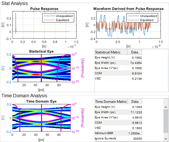
In the SerDes IBIS-AMI Manager accessed from the top level of the receiver block, set the DFE_CDR.ReferenceOffset IBIS-AMI parameter value to 250 (ppm) and rerun the simulations for the First Order Mueller-Muller Loop Filter and the Second Order Mueller-Muller Loop Filter. In the results you observe that the clock time for the First Order Mueller-Muller Loop Filter occurs 5ps later in the eye diagram, and the eye height at the clock time is reduced from 114mV to 107mV.