Channel Operating Margin (COM) for Serial Link
This example shows how to use the channel operating margin (COM) metric within a Serial Link Designer project that has an interface that operates at 100 GT/s per Lane with NRZ modulation. COM is a figure of merit for a passive channel that gives you insight into the quality of the channel design. To calculate COM, use the ratio of signal amplitude factors to noise amplitude factors. Several factors such as channel bit rate, insertion loss, return loss, cross-coupling, transmitter and receiver equalization, and IC package models are applied to determine COM. COM is a valuable part of channel design methodology in general and is required for compliance in some applications such as IEEE 802.3 and OIF CEI standards. For more information on how to calculate and set up COM and how to interpret COM results, see Channel Operating Margin (COM).
The IEEE® 802.3ck defines the channels operating at 106.247Gbps PAM4 meaning a symbol rate of 53.124Gbaud. These channel designs can involve PCB only, backplane, or copper cables. Signaling is accomplished with either NRZ (Non-Return to Zero) or PAM4 (Pulse Amplitude Modulation Level 4). Encoding the packets with forward error correction (FEC) is optional but can greatly improve a channel BER (Bit Error Ratio). Testing the compliance of the passive electrical channel to the specification requires it to meet or exceed COM as measured in decibel units.
COM Example Project
This example references the implementation kit COM_100G_KR, which is a Serial Link Designer project consisting of a 100 Gbps per-lane design. This can be also applied to various IEEE 802.3 and OIF CEI as well as general channel design methodology.
openSignalIntegrityKit("COM_100G_KR");

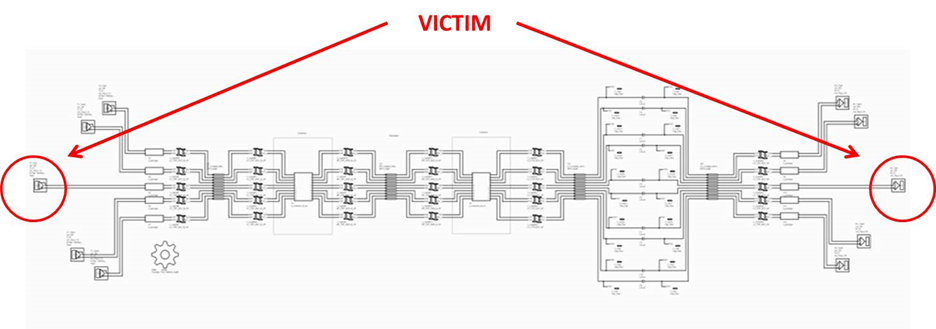
The channel design consists of 5 transmitters and 5 receivers connected with high-speed connectors. The schematic sheet varies aggressor spacing to demonstrate the effects of crosstalk. TX and RX s-parameter package models are included on the schematic sheets. Thus, package characteristics are included in the channel s-parameter models that are passed into COM. The spreadsheet is edited to exclude any package model from the COM calculation as it is part of the channel model.
Running COM in MATLAB
Step 1: Identify Victim Channel
After readying the channel design for simulation and identifying the spreadsheet and reported results, you can start the process of running COM from within the Serial Link Designer app. You need to first identify the victim channel on each of the schematic sheets being simulated. Serial Link Designer creates the appropriate s-parameter files for the victim and any aggressors. To identify the victim channel, edit the Designator Element Properties on the schematic sheet.

To edit the designator element properties, double click on any one of the TX or RX designators on the sheet and open the Designator Element Properties dialog box. Confirm that the Report option is selected for the RX designator of the victim channel only and deselected for any other RX designators. The app automatically determines the FEXT and NEXT aggressor channels based on their position on the schematic sheet with respect to the victim. In this case, the RX3 designator is defined as the victim.

Step 2: Set Simulation Parameters
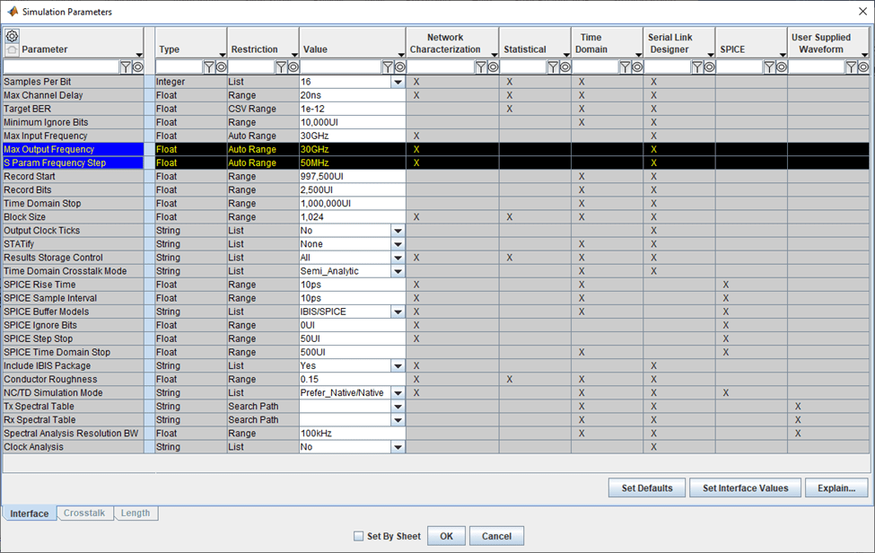
You must set the appropriate simulation parameters in Serial Link Designer before running simulations. The extracted s-parameter models for use in COM must have the necessary bandwidth and frequency spacing to get an accurate representation. These parameters are based on the characteristic delay and the channel bit rate. The parameters affected are Max Output Frequency and S Param Frequency Step.
The Max Output Frequency parameter should be at least two times the fundamental, or Nyquist, frequency based on the channel bit rate (NRZ signaling). For example, if the channel simulations are based on 106.247Gbps PAM4, the Nyquist or fundamental frequency would be approximately 25GHz. The output frequency should then be set to at least 50GHz. This example uses 60GHz for additional margin.
The S Param Frequency Step setting is based on the through-path delay of the channel can be used to calculate the step size. The calculation is based on a settling time of three round trip delays for reflected signal energy.
To edit the simulation parameters, click Setup > Simulation Parameters... to open the Simulation Parameters dialog box.

Step 3: Simulate Schematic Sheet
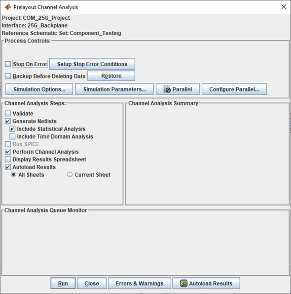
You must simulate the schematic sheet(s) so that Serial Link Designer can generate the necessary s-parameter models for COM. You only need to run network analysis to create the models. To simulate a selected schematic sheet, click Run > Simulate Selected from the Serial Link Designer app toolstrip, then click the Run button in the pop-up window.
Step 4: Set Up COM
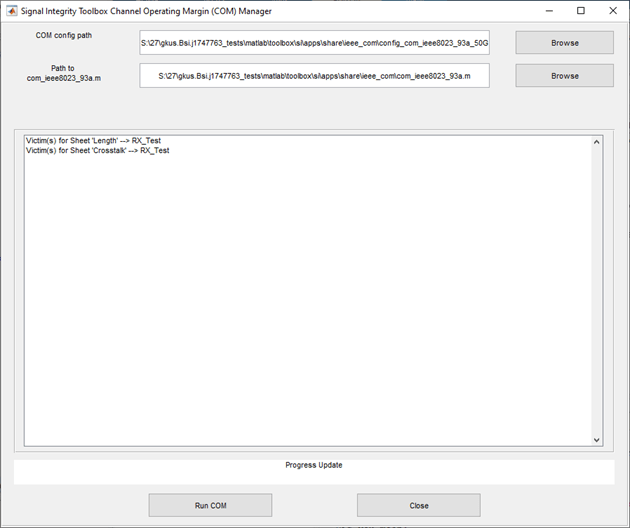
After simulations are complete, click Tools > Run COM Interface. This launches the COM interface in MATLAB®. Select the COM configuration spreadsheet and the COM code.

The COM config path is the spreadsheet configured in Step 1 containing the COM parameters. For this example, get the COM files from the IEEE working group or use example files installed with the Signal Integrity Toolbox™. To use the COM files shipped with Signal Integrity Toolbox, navigate to the matlab\<release>\toolbox\si\apps\share\ieee_com folder of your installation and look for the MATLAB and Excel® files. The COM config is a spreadsheet containing the COM parameter values and COM config path should be set to config_com_ieee8023_93a_3ck_d1p3_KR_09_01_2020.xlsx. The com_ieee8023_93a file is located the same location of your MATLAB installation. Set the Path to com_ieee8023_93a to com_ieee8023_93a_295.m in that folder location.
Note: This file is named com_ieee8023_93a_295.m, which is a local filename and represents COM script version 2.95. The actual files available from the IEEE 802.3 Working Group are each named com_ieee8023_93a.m regardless of version, so keep this in mind for reference (for example, this is the reference name used in the dialog window).
Step 5: Run COM Script and View Results
Click the Run COM button. As the code runs the status is reported in the MATLAB Command Window.

Note: The example runs five separate simulations by sweeping the length. First three of these five cases fail, which is expected and shows the usefulness of sweeping parameters to achieve desired results.
Once the COM simulation is complete, the Signal Integrity Viewer app opens automatically. The Network, Statistical and Time Domain tabs (if simulated) in the Signal Integrity Viewer app all contain the selected results from the COM simulation. You can then select to plot the results you are interested in.
Plotting COM Results
In waveform mode in the Signal Integrity viewer, click on the Statistical tab. Click on the row with the desired value of COM, then right click to see the plotting options. For this example, click the Show Statistical Eye option to observe the statistical eye diagram. Click Show Bathtub > All to view the bathtub curves, clock PDF, and Net BER. You can select and delete any display to focus on the plots you are interested in. You might need to click Display > Refresh to properly see the changes you made to plot.

To save the results in your desired directory, click File > Save Configuration from the Signal Integrity Viewer app toolstrip.
To reopen your saved results, click Tools > Signal Integrity Viewer in the Serial Link Designer app toolstrip, then click on File > Open Configuration from the Signal Integrity Viewer app toolstrip.
The channel COM and other results reported by the COM code are given as single data points. The single value of the COM result in particular makes it easy to determine the pass/fail behavior. If you want to investigate the dependent and independent variables of the simulation results, as they pertain to COM, you can use the Plots tab in the Signal Integrity Viewer app. Using the plots mode, you can uniquely analyze results and create custom plots of virtually any parameter, variable, or result from the simulation. It is an invaluable feature for analyzing large numbers of simulations with many variables. You can define multiple variables and plot them against each other on the x- or y- axis. You can gain greater insight into the channel or system design, especially with very large databases. Identifying trends and finding outliers in the results along with custom plots creation can be the key to a successful design.
References
[1] IEEE P802.3ck 100 Gb/s, 200 Gb/s, and 400 Gb/s Electrical Interfaces, https://www.ieee802.org/3/ck/public/tools/index.html
[2] COM Configuration Documentation: config_com_ieee8023_93a_doc.pdf.