Post-Layout Verification of PCIe 5.0 Allegro Board
This example shows you how to analyze a printed circuit board created in Cadence® Allegro, analyze multiple PCIe 5.0 lanes to determine which will have open or valid eye diagrams, and how to isolate and diagnose lanes with closed eye diagrams by back drilling vias. You can import the board, set it up for simulation by assigning parts, use EBD files for loopback boards, simulate at PCIe 5.0 data rate of 32 Gbps, and finally debug to fix a closed eye diagram.
Get CAD Artifacts for a Post Layout Project
You will see in this example how to create a new project in the Serial Link Designer app. But first, to model a real-world workflow you would have CAD database files representing a PCB layout at this point. To prepare this step, you can download the supporting files for this example using openSignalIntegrityKit to get the archive "post_layout_allegro.zip" that contains the source CAD files to support the workflow shown in this example.
In the MATLAB console, type the following:
>> openSignalIntegrityKit("post_layout_allegro", DownloadOnly=true)
You can now unzip post_layout_allegro.zip in a working folder for your new project.
Note: You can also use openSignalIntegrityKit to get many industry-standard kits which include pre-configured transmitter and receiver IBIS-AMI models as well as specification compliance rules such as Eye Masks, dB margin analysis using S-Parameter Network plots, and support for analysis using Channel Operating Margin (COM and eCOM).
Create New Project
Now that you have the artifacts representing CAD data for a PCB layout along with a blank project, you can also see how to create a new project in Serial Link Designer by opening the app by typing the following into the MATLAB console:
>> serialLinkDesigner
In Serial Link Designer you can create a new project by selecting File > Project > New Project. In the newly opened dialog box, name the project as post_layout and the interface as PCIe and click OK. Click the Post-Layout Verification tab which shows a blank page.
Import IBIS-AMI Model
Use the IBIS-AMI model included with this example for the post-layout verification of the board. The IBIS-AMI model represents the PCIe 5.0 SerDes in the ASIC that is on the board. The AMI portion of the model is generated using the SerDes Toolbox™ and the PCIe 5.0 specification.
To import the IBIS-AMI model, select Libraries > Import IBIS then navigate to the folder that contains the IBIS-AMI file named asic.ibs, then click Import.
Setup and Assignment
To import the boards, in the Post-Layout Verification tab, click the Setup & Assignment button in the Post-Layout Operations section. This opens the Post-Layout Setup & Assignment window.
Import & Setup Boards
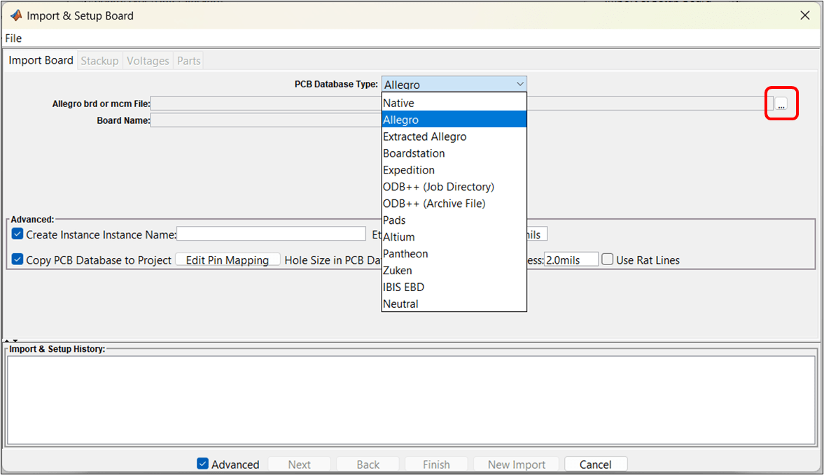
First, import and set up the main board that has the ASIC and into which all other boards will plug. In the Post-Layout Setup & Assignment window, click the Import & Setup Board button in the Boards section.
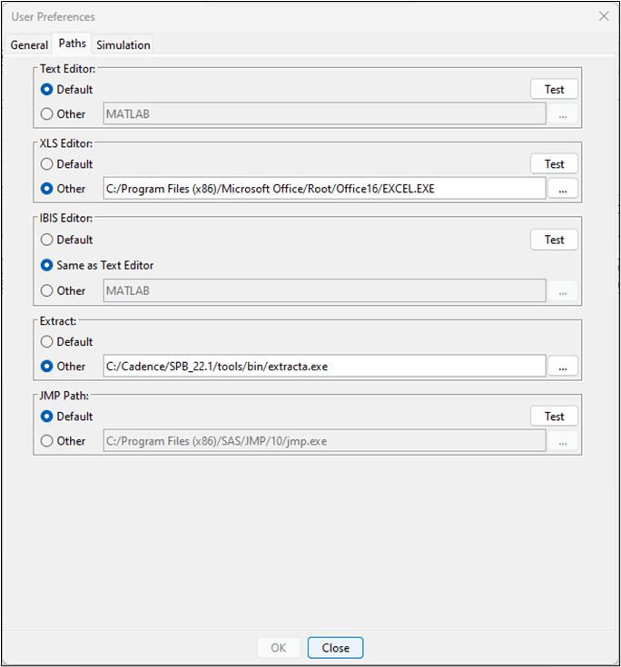
You can import PCB databases created in a variety of different PCB CAD software. In this example, the main board was created in Allegro and is named PCIe_board.brd. If you have Allegro installed on you computer, you can import Allegro boards. To enable the import of Allegro boards, click Setup > User Preferences. In the User Preferences window, click the Paths tab and under Extract, point to extracta.exe in the Cadence folder. If you do not have Cadence installed, skip down to install the Native file instead.
Select Allegro from PCB Database Type parameter. To select the PCIe_board.brd file, navigate to the unzipped post_layout_allegro folder from Allegor brd or mcm File parameter and select it. Select the Advanced option in the Import and Setup Board dialog box.
The Board Name and Create Instance Name parameters are automatically filled with the file name of the board. For files with longer board names and instance names, you can rename them to make them shorter.
Click Next to import the board.
If you do not have Allegro installed, you will import a Native PCB Database instead. Select Native in the PCB Database Type pull down menu and navigate to the unzipped post_layout_allegro > native folder from pins.csv file parameter and select pins.csv. Select the Advanced option in the Import and Setup Board dialog box.
Click Next to import the board.
Note: A warning appears saying that the dielectric constants for various layers have been changed during the import process. Click OK because the next step tells you to check the board stackup.
After importing the board, you should always check the board stackup to make sure it is correct. Check that the layer thicknesses, dielectric constants, and loss tangents for all the layers are what you expect them to be. After you have verified the stackup to be correct, click Next.
The next step is to verify the voltages on the board. This step is important for simulations that requires the use of the voltages on various nets of the board, such as DDR simulations. For this example, the voltages of the nets is not used so you can click Next.
The last step of the Import & Board Setup process is to assign parts. Click on the # Pins column heading to sort the pins from largest to smallest. The ASIC or FPGA is usually the part with the greatest number of pins and will have a RefDes of U1. When you have found the ASIC, right-click on it and select Part > Browse to assign the asic.ibs file you imported earlier.
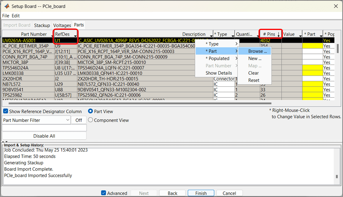
Finally, click on Type to find the capacitors on the board. Assign a value of 22 μF to the capacitors. Click Finish to complete setting up the board.

Repeat these steps to import the CXL_loopback.ebd and PCIe_loopback.ebd boards. These two boards do not have a stackup, voltages, or parts associated with them. They are only used to connect a transmitter (Tx) to its associated receiver (Rx), both of which are on the ASIC. The CXL_loopback.ebd plugs into the 26 CXL connectors on the board and the PCIe_loopback.ebd plugs into the two PCIe connectors.
View Board
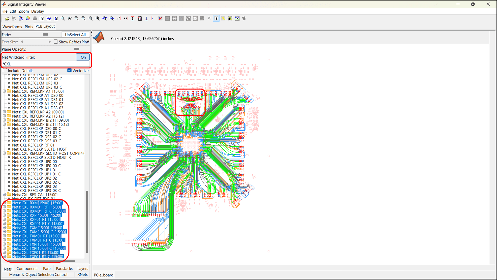
To view the PCIe_board, right-click on the PCIe_board in the Boards section of the Post-Layout Setup & Assignment window. The Signal Integrity Viewer app opens and defaults to the Nets tab. While in the Nets tab, select the option Vectorize.
To view all of nets on the board, shift-click all the nets. This view shows all the nets, whether they are set to be simulated or not. To view only the nets you are simulating, in the box under Net Wildcard Filter:, enter *CXL and then click the Off button to turn on the filter.
Scroll to the bottom of the list of nets and shift-click all the nets that begin with CXL_RXM, CXL_RXP, CXL_TXM, and CXL_TXP. These are the high-speed nets that runs the PCIe 5.0 signals. The ASIC is in the middle of the board with the CXL connectors surrounding the ASIC and the two PCIe connectors are at the bottom left of the board.
Note: The nets just above the ASIC, in the red box shown below, are nets that have a retimer between the connector and ASIC. Since a retimer is not included in the example, these nets will not be simulated.
Instances
When you import the asic.brd, CXL_loopback.ebd, and PCIe_loopback.ebd, an instance is created for each board. An instance is an internal copy of a board that you can connect to other instances. Every board that is used in the design has at least one instance. If you use the same board more than once, you must define a separate instance for each use. In this example, you need to create a total of 26 instances of the CXL_loopback board and two instances of the PCIe board. You can do this by selecting the CXL_loopback instance and click Add Instance. Repeat until you have 26 CXL_loopback instances in total. Do this again so you have two instances of the PCIe_loopback.

Connections
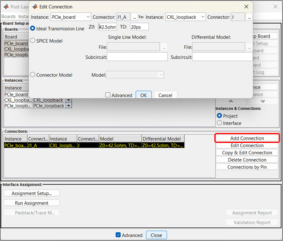
The final step in the Setup process, before running assignment, is to connect all the boards to each other. Click Add Connection to open the Edit Connection window. Here you can connect one board to another via connectors on each board. You have a choice of what to use to connect the boards: Ideal Transmission Line, SPICE Model, or Connector Model. If you want to use either a SPICE Model or Connector Model (measured or simulated S-parameters in a Touchstone File), you need navigate to the model in the project folder. For this example, you will use an Ideal Transmission Line.
You need to connect the 26 CXL_loopback instances and the two PCIe_loopback instances to the PCIe_board instance. Therefore, in the first Instance dropdown menu. select the PCIe_board instance. In the first Connector dropdown menu, select connector J1_A. In the second Instance dropdown menu, select CXL_loopback, and in the second Connector dropdown menu, select connector J. For the Ideal Transmission Line, use a reference impedance (Zo) of 42.5 ohms and an electrical length or time-delay (TD) of 20 ps. When finished, click OK.
You just connected the connector with the reference designator of J1_A on the PCIe_board to connector J on the CXL_loopback board via a 42.5 ohm transmission line with an electrical length of 20 ps.
Repeat this process to connect the remaining 25 CXL loopback instances and the two PCIe loopback instances to their respective CXL and PCIe connectors on PCIe_board. The reference designators of the connectors on the PCIe_board and the loopback instance are:
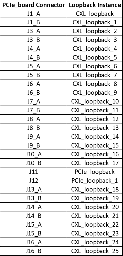
Note: Skip the connectors with the reference designators J2_A and J2_B. Those two connectors are part of nets that have a retimer between the connector and ASIC and thus is not simulated. Also, connectors J11 and J12 are the two PCIe connectors on the PCIe_board.
Run Assignment
After making and checking all of the connections, run assignment. The assignment process is an automated process for associating nets in the PCB database with transfer nets. Click the Run Assignment button in the Interface Assignment section. Review the Assignment Report and Validation Report, then click Close in the Post-Layout Setup & Assignment window.
Set Transfer Net Properties
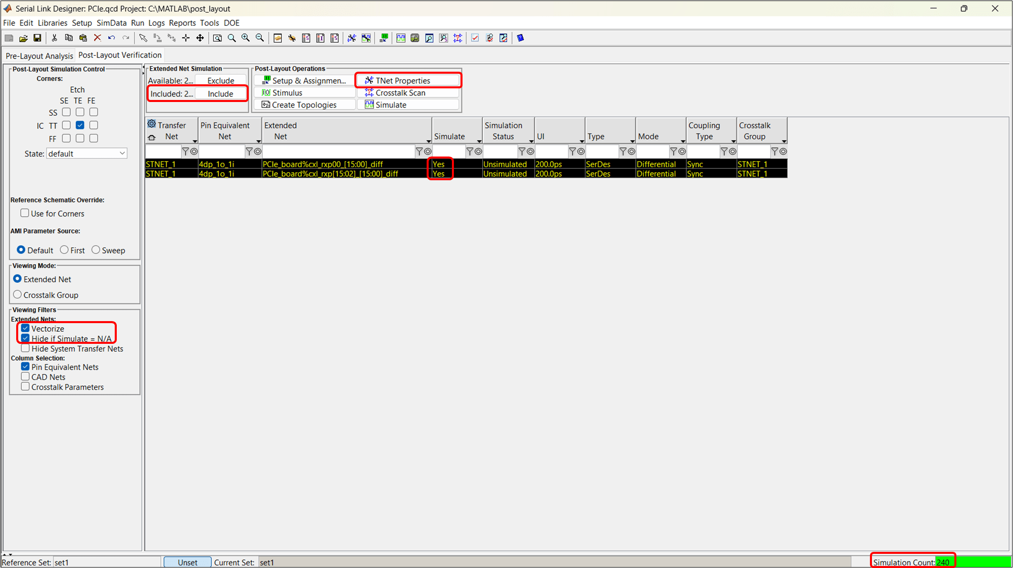
When you get back to the Post-Layout Verification tab of the Serial Link Designer app, select the Vectorize and Hide if Simulate = N/A options. Selecting the Vectorize option groups the extended nets of similar names to make viewing easier. The extended nets PCIe_board%cxl_rxp00_[15:00]_diff are associated with the CXL_loopback instance and connectors J1A and J1B. The extended nets PCIe_board%cxl_rxp[15:02]_[15:00]_diff are associated with the remaining instances and connectors. Since you skipped connectors J2_A and J2_B, the Vectorize process skipped PCIe_board%cxl_rxp01_[15:00]_diff. Since this extended net was skipped, you can see two rows of exteneded nets. Otherwise, there would have been just one row of Extended Nets, PCIe_board%cxl_rxp[15:00]_[15:00]_diff. This is how the Vectorize process works.
You are only simulating a portion of the board, only those nets that will run PCIe 5.0 signals. Selecting the Hide if Simulate = N/A option removes unsimulated nets that do not run PCIe 5.0 signals.
Select the two rows of Extended Nets and click Include in the Extended Net Simulation section. This includes all of the extended nets when you run the simulation, totalling to 240 simulations, as shown in the bottom right corner of the Serial Link Designer app. It also changes the No to Yes in the Simulate column for each row of extended nets.
If you only want to simulate a subset of extended nets instead of all 240, click Exclude in the Extended Net Simulation section to remove all of the extended nets from simulation, uncheck the Vectorize box to see all of the individual extended nets, select only the extended nets you want to simulate, and then click Include.
When you have selected the extended nets you wish to simulate, click the TNet Properties button in the Post-Layout Operations section.
Transfer Net Properties
Now set the Source and Target as well as set the data rate for PCIe 5.0.
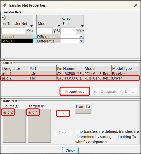
In the Transfer Net Properties window, select the Source and Target and then click the arrow. In this example, there is only one Source and one Target to choose from.
Select the Tx Driver and click the Properties button to set the data rate for the simulation.
To set the data rate in the Designator Element Properties window, use the dropdown menu in the UI column to choose the appropriate data rate and unit interval. The PCIe 5.0 data rate is 32 Gbps and has a UI of 31.25 ps but these are not listed in the dropdown menu. To add them to the list, click the Edit Clock Domains button in the Designator Element Properties window.
A text file will open in MATLAB that contains all of the built-in data rates and unit intervals. In the section that has all of the SerDes data rates, add a row and then add SerDes_32G = 31.25ps, then click Save and close the file.

When you get back to the Designator Element Properties window, use the dropdown menu in the UI column and the PCIe 5.0 data rate and unit interval will now be available. Choose 31.25ps - SerDes_32G and click Close.
If you have multiple, different extended nets, it is recommended to rename the transfer nets to something more appropriate than the default STNET. When you are back in the Serial Link Designer app, select the two rows of extended nets, right click on them, select Rename Transfer Net, and change the transfer net names to PCIe.
Before simulating the board, click on the Pre-Layout Analysis tab in the Serial Link Designer app. There are two sheets: the original sheet that was made when the Project was created and the PCIe sheet that represents the Transfer Nets from the Post-Layout Verification tab. Right click and remove the original sheet and include the PCIe sheet for simulation.

Simulation
Click Simulate in the Post-Layout Operation section to open the Post-Layout Channel Analysis window.
If you have Parallel Computing Toolbox™ or MATLAB Parallel Server™, click the Parallel button to perform multiple simulations simultaneously. If using the Parallel Computing Toolbox, you can use each core of your CPU to run one simulation.
In the Channel Analysis Steps section, select these options: Validate, Generate Netlists, Include Statistical Analysis, Perform Channel Analysis, and Autoload Results. To save time, skip the time-domain analysis. Click Run.
Results
When the simulation is complete, the Signal Integrity Viewer app opens automatically.
In the bottom left corner of the Signal Integrity Viewer app, you see two tabs, 0: Network and 1: Statistical. Each row in the solution space represents one simulation. View the results in the solution space for each tab by scrolling up or down for each simulation and left or right to see the results.
While on the 0: Network tab, select all of the simulations by shift-clicking the first and last row and then right-click on any of the rows. This opens a menu allowing you to plot various waveforms. Select Show S-Parameters (DB) > Mixed Mode Thru-Path (Insertion Loss) > DD to view all 240 differential insertion loss waveforms in one plot. When doing so, notice a large resonances between 15 - 20 GHz.
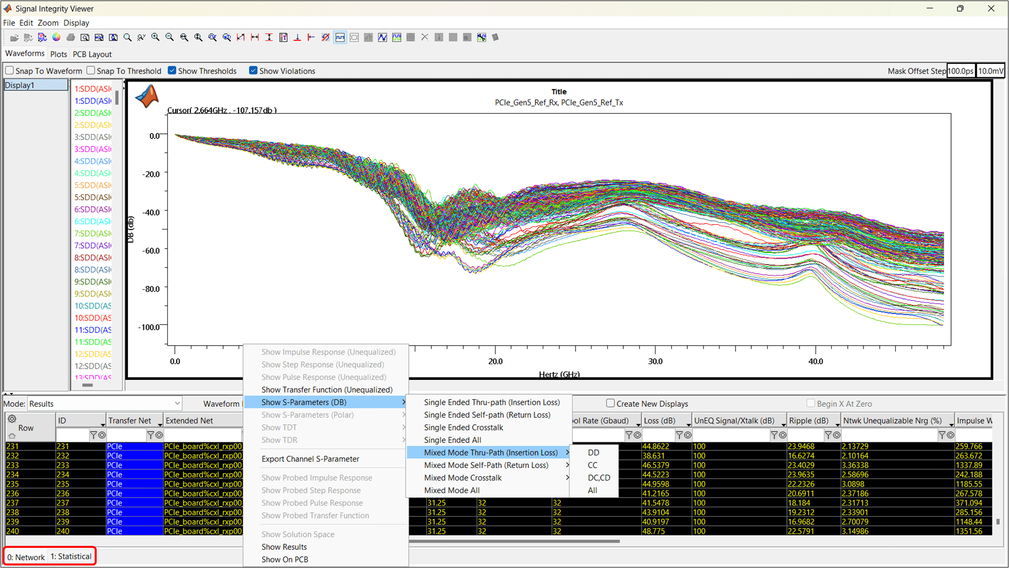
Click Display > Add Display Panel to add a new blank display. While on the 1: Statistical tab, right click on one simulation row and Show BER to view the eye diagram, bathtub curve, and clock PDF. You can see that the eye is closed, which is expected due to the large resonance between 15 - 20 GHz you noticed before, right where the Nyquist frequency happens to be.

Investigation of Post-Layout Verification Results using Post-to-Pre-Layout Simulations
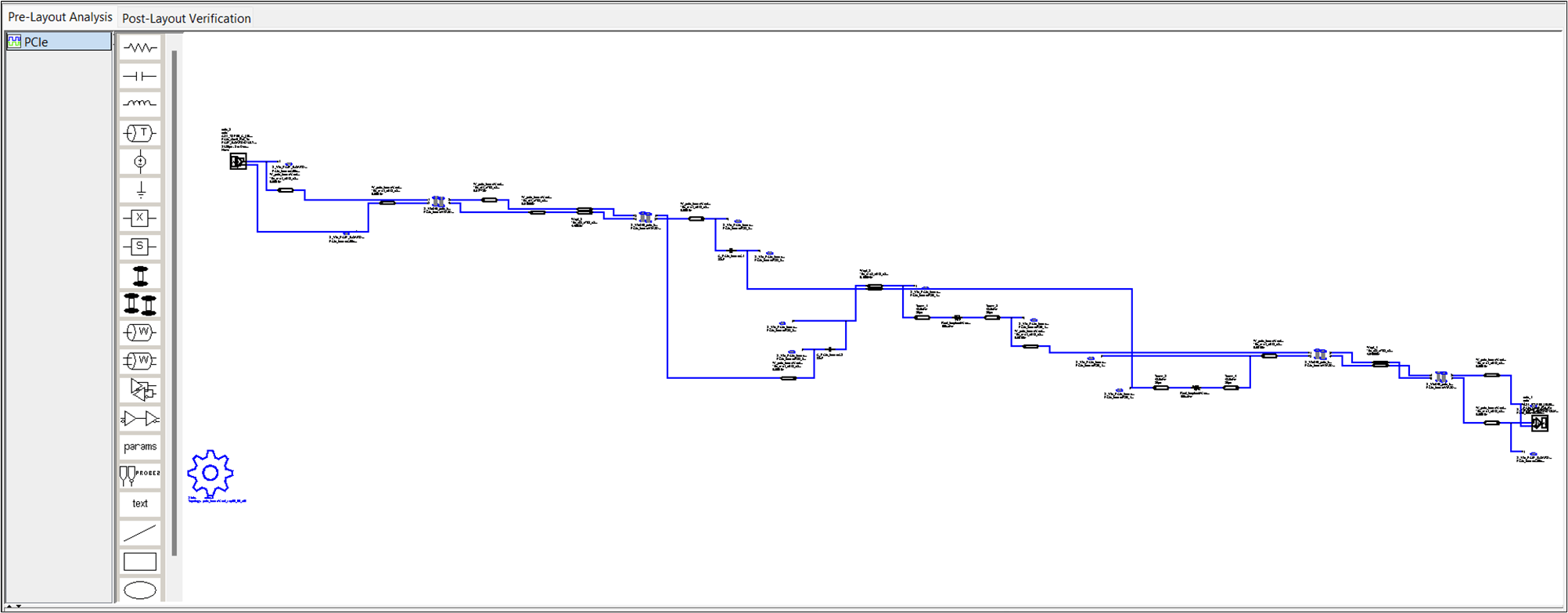
To investigate the cause of the resonances and resulting eye closure, you can create a post-to-pre-layout topology of the board (e.g. extract a post-layout Xnet to pre-layout canvas schematic). Extracting post-layout to pre-layout allows you to look more closely at lossy transmission lines, vias, lumped element model values, and other items.
From the Post-Layout Verification tab of the Serial Link Designer app, select the extended nets and click Create Topologies.
To view an extended net as a pre-layout topology, double click the gear icon in the Pre-Layout Analysis tab and select the desired extended net.
Note: The nomenclature is pre-layout, but this is in fact an extracted topology from the post-layout design that was imported in earlier steps.
You can double click or right click on elements to investigate the design as shown:
Investigate Via Designs using Pre-Layout Simulations
For this example, investigate the differential vias using the post-to-pre-layout extracted topologies.
Note: In this section of the example, you are working in the pre-layout schematic flow, which does not affect the actual layout or post-layout extracted nets availabe on the Post-Layout Verifcation tab. Any changes here would have to either be made manually as follows:
Option 1: Make changes in the Post-layout Via Library Editor and re-run Assignment.
Option 2: Or, make equivalent change the original PCB design and then re-import that design.
In the meantime, you can investigate the effects of design metrics as follows.
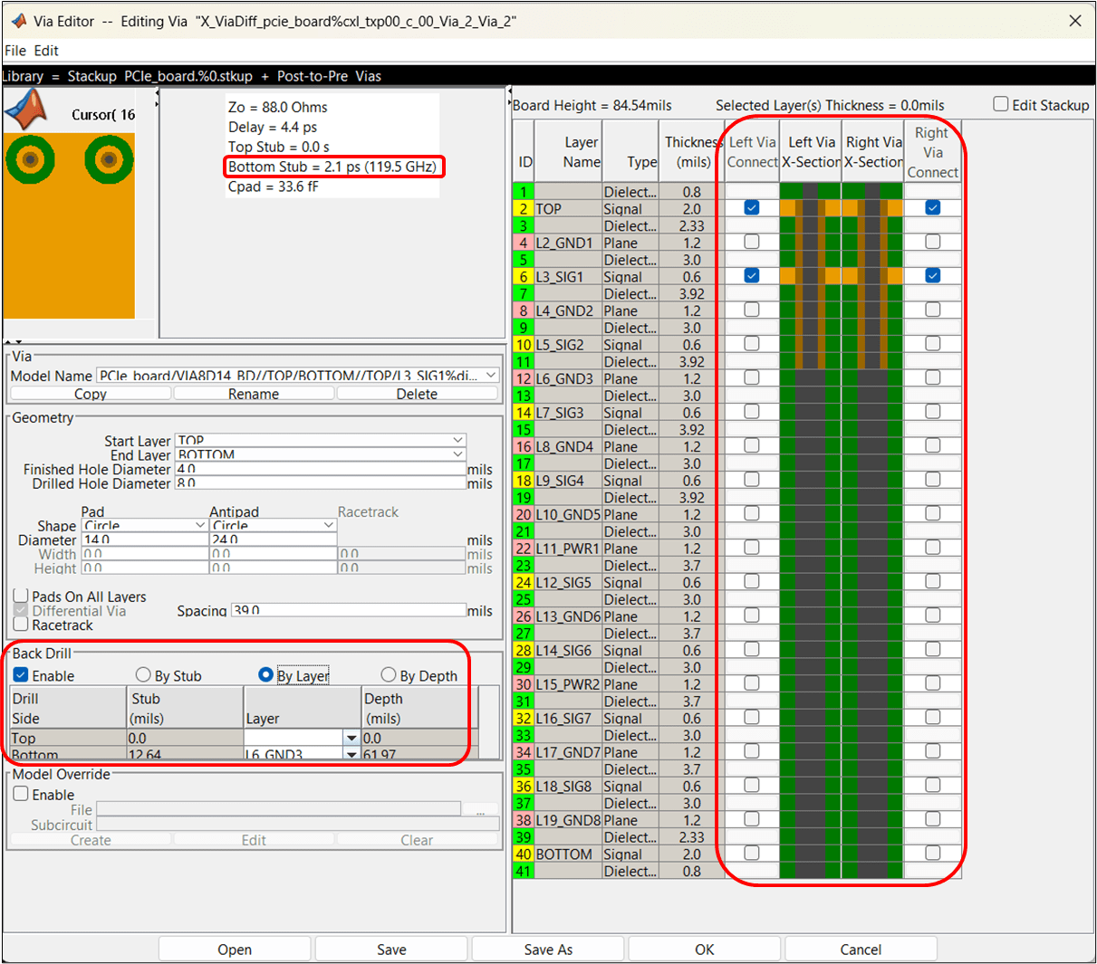
Starting with the differential vias on the left, closest to the Tx, right click and chose Edit Differential Via Model to open the vias in the Via Editor.
In the cross-sectional view in Via Editor dialog box, notice that these vias are not backdrilled. Also notice that the Bottom Stub has an electrical length of
12.9 pswhich corresponds to a resonance at19.3 GHz. You saw this resonance in the insertion loss waveforms earlier. Therefore, the solution is to backdrill the vias.

There is a note with the Allegro board file that says vias that are routed on Layer 3 (Signal Layer 1) are to be to back drilled to Layer 6 (Ground Layer 3). To back driil the vias, select the Enable option in the Back Drill section, and back drill By Layer to
L6_GND3. The cross-sectional view updates to show the back drilling. The Back Drill section that the Stub (mils) and Depth (mils) columns also automatically updates with the value of12.64and61.97respectively. The Bottom Stub value decreases from12.9 psto2.1 pswhich pushes the resonance out to119.5 GHz, which is well outside the frequencies of interest.When you are finished reviewing the back drilling options, click Save and Close.
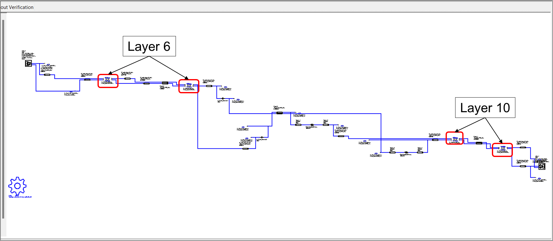
Since there are three more sets of differential vias, you need to repeat this process three times more to back drill them to their desired layers.
Going from left to right, back drill the second set of vias to Layer 6 and the third and fourth sets of vias to Layer 10.
Next, simulate the one extended net and view the differential insertion loss and eye diagram. Notice that the resonance is now gone and the eye is now open.


You have seen in this example how to perform post-layout extraction, and how to import post-to-pre-layout in order to investigate design metrics such as via back-drilling.
Note: It is important to remember that post-layout extraction tab Xnets are derived from the actual PCB database:
Notes Regarding Post-Layout Analysis, Pre-Layout Analysis, and Post-to-Pre-Layout Extraction
Post layout Xnets are derived firstly from PCB extraction during import.
Post layout Xnets can be modified using imported S-Parameter Touchstone files or modified using the via-editor or t-line editor, as appropriate.
However, Assignment must be re-run to instantiate any design changes for post-layout analysis.
Post-to-Pre-Layout is a workflow provided to enable investigation of Xnets with regards to Via design and T-line or W-element design conisiderations. These changes are not reflected unless also made as changes either in the original PCB design and re-imported, or as changes to the Via or T-line/W-line element library and re-running Asssignment.
Note: Changes meant for Post-Layout analysis require re-running Asssignment in order to re-generate simulation libraries.
Pre-Layout is always available as a means to provide "from-scratch" investigation of design concerns regarding vias and T-line/W-line elements for your design. Assignment does not have to be re-run for items modified on a schematic sheet canvas.
Elements modified on Pre-layout sheets are often database-atomic to that canvas or by filename if used in multiple canvases (e.g. such as the case of W-line model files).