主要内容

New FPGA Board Wizard

R2026b

Create, configure, and add custom board for FPGA-in-the-loop workflows

Description

The New FPGA Board Wizard steps you through the workflow to enter the required information to add a board to the FPGA board list. This list applies to FPGA-in-the-loop (FIL) workflows.

Before adding an FPGA board, review FPGA Board Requirements to make sure that it is compatible with the workflow you want to use.

Add Boards Once for Multiple Users.  To add new boards globally, follow these steps:

  1. Create the following folder:

    matlabroot/toolbox/shared/eda/board/boardfiles

  2. Copy the board description XML file to the boardfiles folder.

  3. After copying the XML file, restart MATLAB®. The new board appears in the FPGA board list for the FIL workflow.

Note

To access a board added globally, all users must be using the same MATLAB installation.

All boards under this folder appear in the FPGA board list automatically for users with the same MATLAB installation. You do not need to use FPGA Board Manager to add these boards again.
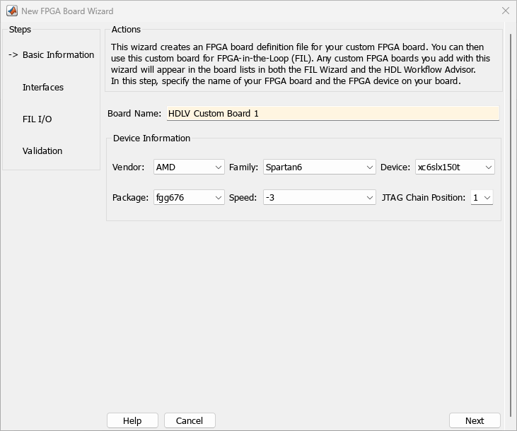
New FPGA Board Wizard

Open the New FPGA Board Wizard

Parameters

expand all

Basic Information

Specify a unique name for your custom board. This name appears in the board list of the FPGA Board Manager.

Select the vendor of your board.

Specify device-specific properties.

  • Family — The device family depends on the specified vendor. See the board specification file for applicable settings.

  • Device — See the board specification file to select the correct device.

  • For AMD® boards only:

    • Package — See the board specification file to select the correct package.

    • Speed — See the board specification file to select the correct speed.

    • JTAG Chain Position — This value indicates the starting position for JTAG chain. See the board specification file for this information.

Interfaces

To enable FPGA-in-the-loop, select FIL Interface. Then, select one of the following options under PHY Interface type:

For Intel (Altera) Boards

  • Altera JTAG

  • Gigabit Ethernet — GMII

  • Gigabit Ethernet — RGMII

  • Gigabit Ethernet — SGMII

  • Ethernet — MII

For AMD Boards

  • JTAG

  • Gigabit Ethernet — GMII

  • Gigabit Ethernet — AMD SGMII

  • Gigabit Ethernet — AMD SGMII with 625MHz Reference Clock

  • Ethernet — RMII

  • Ethernet — MII

  • Ethernet — MII with 25MHz Output

For more information on how to set up the JTAG connection for AMD boards, see Interface.

Note

Not all interfaces are available for all boards. Availability depends on the board you selected in the Basic Information section.

Limitations

When you simulate your FPGA design through a Digilent® JTAG cable, you cannot use any other debugging feature that requires access to the JTAG interface. For example, the Vivado® Logic Analyzer.

To configure your board, you must provide clock details. You can find all necessary information in the board specification file (available from the board vendor).

  • Clock Frequency — Must be from 5 through 300. For an Ethernet interface, the suggested clock frequencies are 50, 100, 125, and 200 MHz.

  • Clock TypeSingle_Ended or Differential.

  • Clock Pin Number (Single_Ended) — Must be specified. Example: N10.

  • Clock_P Pin Number (Differential) — Must be specified. Example: E19.

  • Clock_N Pin Number (Differential) — Must be specified. Example: E18.

  • Clock IO Standard — The programmable I/O standard to use to configure input, output, or bidirectional ports, for example, LVDS.

To indicate a reset, find the pin number and active level in the board specification file, and enter that information.

  • Reset Pin Number — Leave empty if you do not have one.

  • Active LevelActive-Low or Active-High.

  • Reset IO Standard — The programmable I/O standard to use to configure input, output, or bidirectional ports, for example, LVCMOS33.

FIL I/O

Provide the FPGA pin numbers for the specified signals. You can find this information in the board specification file. For vector signals, list all pin numbers on the same line, separated by commas.

Tip

If your PHY chip does not have the optional TX_ER pin, tie ETH_TXER to one of the unused pins on the FPGA.

Management Data Input/Output (MDIO) is a serial bus, defined in the IEEE® 802.3 standard, that connects MAC devices and Ethernet PHY devices. The FPGA MAC uses the MDIO bus to set control registers in the Ethernet PHY device on the board.

Currently, only the Marvell® 88E1111 PHY chip is supported by this MDIO module implementation. Do not select this check box if you are not using Marvell 88E1111.

The generated MDIO module performs the following operations:

  • GMII mode: The PHY device can start up using other modes, such as RGMII/SGMII. The generated MDIO module sets the PHY chip in GMII mode.

  • RGMII mode: The PHY device can start up using other modes, such as GMII/SGMII. The generated MDIO module sets the PHY device in RGMII mode. In addition, the module sets the PHY chip to add internal delay for RX and TX clocks.

  • SGMII mode: The PHY device can start up using other modes, such as RGMII/GMII. The generated MDIO module sets the PHY chip in SGMII mode.

  • MII mode: The generated MDIO module sets the PHY device in GMII compatible mode. The module also sets the autonegotiation register to remove the 1000 Base-T capability advertisement. This reset ensures that the autonegotiation process does not select 1000 Mbits/s speed, which is not supported in MII mode.

When To Select MDIO: Select the Generate MDIO module to override PHY settings option when both the following conditions are met:

  • The onboard Ethernet PHY device is Marvell 88E1111.

  • The PHY device startup settings are not compatible with the FPGA MAC. The MDIO modules for different PHY modes must override these settings, as previously described.

Specifying the PHY Address: The PHY address is a 5-bit integer. The value is determined by the CONFIG[0] and CONFIG[1] pin on Marvell 88E1111 PHY device. See the board manual for this value.

Dependencies

This option is available only when the onboard Ethernet PHY device is Marvell 88E1111.

Validation

Select this option to generate an FPGA programming file.

Program the FPGA with the generated programming file, detect the Ethernet connection (if selected), and perform FPGA-in-the-loop simulation.

Dependencies

This option is available when Run FPGA-in-the-Loop test is selected.

Use this option for setting the IP address of the board if it is different than the default IP address (192.168.0.2).

If necessary, change the computer IP address to a different subnet from 192.168.0.x when you set up the network adapter. If the default board IP address 192.168.0.2 is in use by another device, change the Board IP address according to the following guidelines:

  • The subnet address, typically the first 3 bytes of board IP address, must be the same as the host IP address.

  • The last byte of the board IP address must be different from the host IP address.

  • The board IP address must not conflict with the IP addresses of other computers.

For example, if the host IP address is 192.168.8.2, then you can use 192.168.8.3, if available.

Dependencies

This option is available for Ethernet interface only, when Run FPGA-in-the-Loop test is selected.

Version History

Introduced in R2012b