Test Harness to Generate High-Power IGBT Device Characteristics
This example provides test harness for estimating switching loss for different parameters of a N-Channel IGBT block.
For more information on designing and analyzing a three-phase converter, refer examples,
TestHarnessNChannelIGBT.ConverterDesign.
To access the overall workflow, click on the hyperlink in the model canvas or, at the MATLAB® Command Window, type:
edit ConverterDesignIGBTWorkflow.mlx
Test Harness for High-Power Converter Switching Loss Estimation
This model plots the variation of switching loss characteristics for these IGBT simulation parameters:
Collector-emitter current

PWM switching frequency

Gate-emitter voltage

Collector-emitter voltage

Gate resistance

Junction temperature

This example plots the IGBT characteristics for both double pulse and sinusoidal PWM gate signals. The IGBT device under test is placed in the lower (IGBTL) leg of a converter. To determine the single turn-on and turn-off characteristics, this model uses a double pulse gate signal. To simulate the voltage  and current
  stress on the IGBT-diode device combination in a typical two level converter, a sinusoidal PWM gate modulation signal is used along with a sinusoidal output collector current. Sinusoidal
  load current with sinusoidal voltage modulation signal option enables you to simulate for different power factor, power frequency, and switching frequency. IGBT characteristics are plotted for both double pulse and sinusoidal PWM gate signals.

Parameter Selection Mask for Switching Loss Estimation Test Harness
To define the simulation parameters and plot the switching loss characteristics, open the right-hand top corner parameters selection mask.

Simulated Switching Loss Characteristics for Single Turn-On and Turn-Off
The IGBT switching loss values change according to the definition of the switching region and on the free wheeling diode. In this example, some of the diode reverse recovery is part of the turn-on switching region and any power loss (Vce*Ice) greater than lossFactor*max(Vce*Ice) is a switching loss. This example uses loss factor of 0.02 (2% of max switching power). During switching, any power loss (Vce*Ice) greater than lossFactor*max(Vce*Ice) is considered as a switching loss.
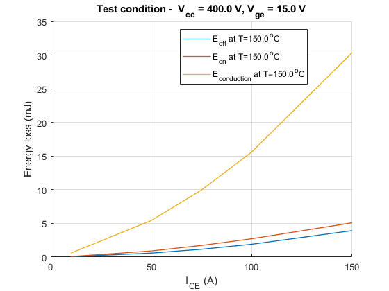
Simulated Loss for Different Ice
This plot shows the simulated loss for different Ice.

Simulated Loss for Different Vce
This plot shows the simulated loss for different Vce.

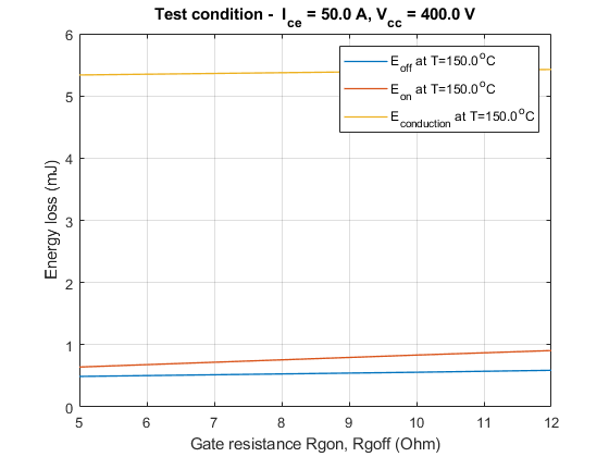
Simulated Loss for Different Rg
This plot shows the simulated loss for different Rg.

Simulated Switching Loss Characteristics for Sinusoidal Load Current and Modulation Signal
Simulated Output for Sinusoidal Load Current This plot shows the simulated output for the sinusoidal load current when  .
.

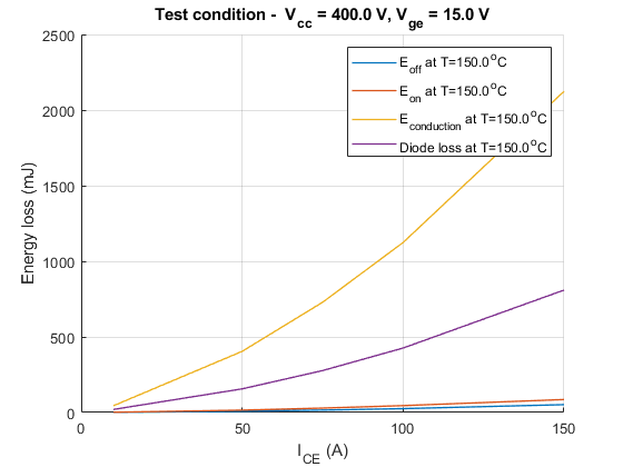
Simulated Loss for Different Ice
This plot shows the simulated loss for different Ice when  .
.

Simulated Loss for Different PWM Frequency
This plot shows the simulated loss for different PWM frequencies.
