Compare DAC Converter Output Signals to Reference Signals on an STM32 Microcontroller Using Comparator Block
This example shows how to use Model DAC and ADC for Signal Conversion on STM32 Processor and Comparator blocks from the STM32 Microcontroller Blockset to model comparisons between digital-to-analog converter (DAC) output signals and reference signals. You can use the blocks in two modes:
Basic mode, which involves one Comparator block
Window mode, which involves two Comparator blocks
Compare DAC Output Signal to Reference Signal
In a model, you can use the DAC block to receive a digital value and convert that value to an equivalent analog voltage on a corresponding channel of the STM32 module. You can use the Comparator block to compare the analog voltage to a reference voltage.
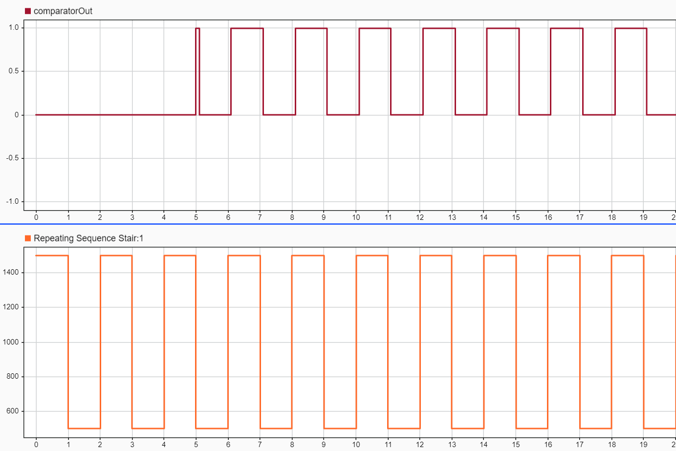
Consider the example model comparatorGettingStarted.slx:
The Repeating Sequence Stair block outputs and repeats a stair sequence, using the vector of values
[1500 500]. A value in the vector is output each second and then the sequence repeats.The DAC block receives the digital value (dIn) from the Repeating Sequence Stair block. The DAC block is configured with default parameter settings with exception of the Channel select parameter, which is set to
Channel2.The DAC block converts the value of dIn to an analog voltage on channel 2.
The Step block initiates a step at 5 seconds (Step time is set to
5) at a sample rate of 0.1.The Data Type Conversion block converts the output of the Step block to type
booleanas specified by the Output data type parameter.The Comparator block compares the analog voltage output of the DAC block to a reference voltage that gets enabled when you select parameter Run time module Enable. The block returns the logical value of the result: 0 if the output voltage of the DAC block is less than the reference voltage or 1 otherwise.
Use STM32CubeMx to specify the comparison mode and required IOC configuration. For example:
Open STM32CubeMx.
In the left pane, select
COMP1.In the right pane, set Input [-], the input voltage (
Vin), to3/4 Internal VRef.
This example assumes these voltage values, which are specified in the IOC file:
The DAC input voltage, Vin, is 1.2 V.
The reference voltage,
Vref, is 0.9 V (.75*1.2).The output voltage is 1117 V (
Vref/Vin*2^(n-1)=(0.9/3.3*4095) )
This Simulation Data Inspector view shows the comparator is enabled at 5 seconds. The 0.1 second shift to the right is to due to the sample time configured for the Comparator block.
Check Whether DAC Output Signal is Within a Specified Window Range
In a model, you can use the DAC block to receive a digital voltage convert the voltage to analog signal, and then use two Comparator blocks to compare the converted signal to reference signals that specify a voltage range (window range). This setup is useful for monitoring when external signals are within a voltage range.
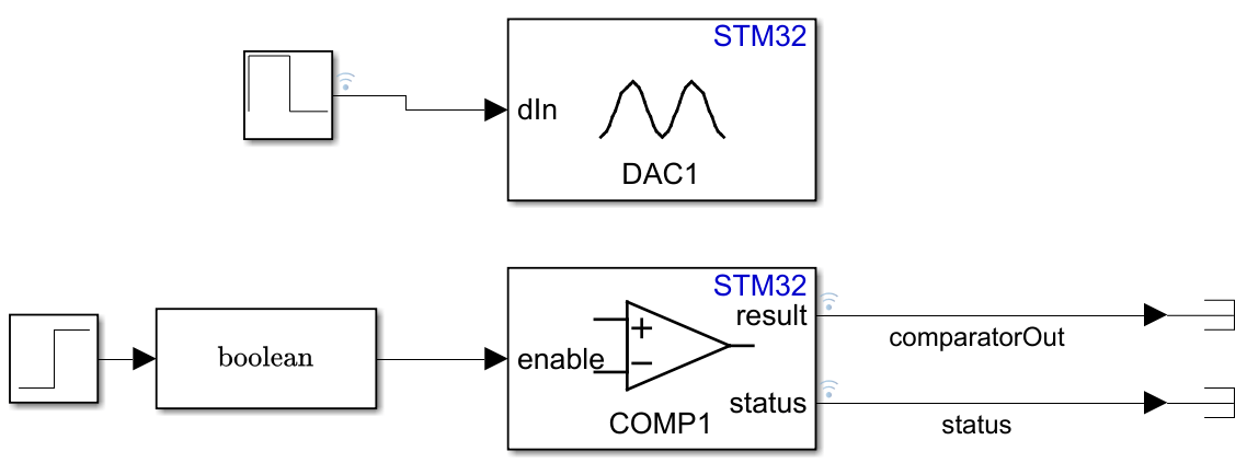
Consider example model comparatorWindowMode.slx:
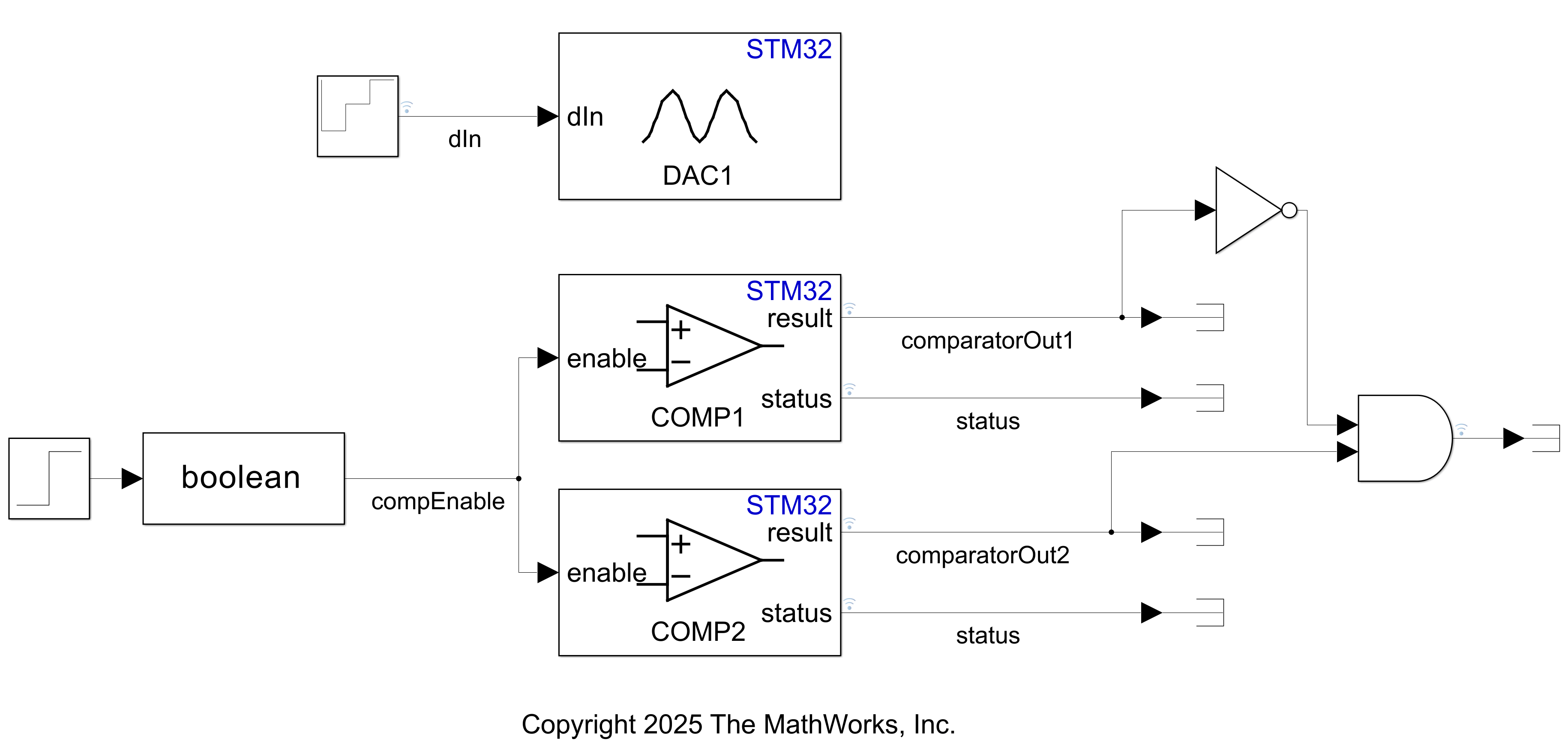
The Repeating Sequence Stair block outputs and repeats a stair sequence, using the vector of values
[500 1000 1500]. A value in the vector is output each second and then the sequence repeats.The DAC block receives the digital value (dIn) from the Repeating Sequence Stair block. The DAC block is configured with default parameter settings with exception of the Channel select parameter, which is set to
Channel2.The DAC block converts the value of dIn to an analog voltage on channel 2.
The output signal of the DAC block is routed to two Comparator blocks.
The Step block initiates a step at 5 seconds (Step time is set to
5) at a sample rate of 0.1.The Data Type Conversion block converts the output of the Step block to type
booleanas specified by the Output data type parameter.The Comparator modules, COMP1 and COMP2, compare the output signal of the DAC block to reference voltages that get enabled when you select parameter Run time module Enable. For each Comparator block, the reference voltage is set internally. The block returns the logical value of the result: the values of
Vref1and Vref2. The voltage is considered high if the DAC output voltage is betweenVref1andVref.
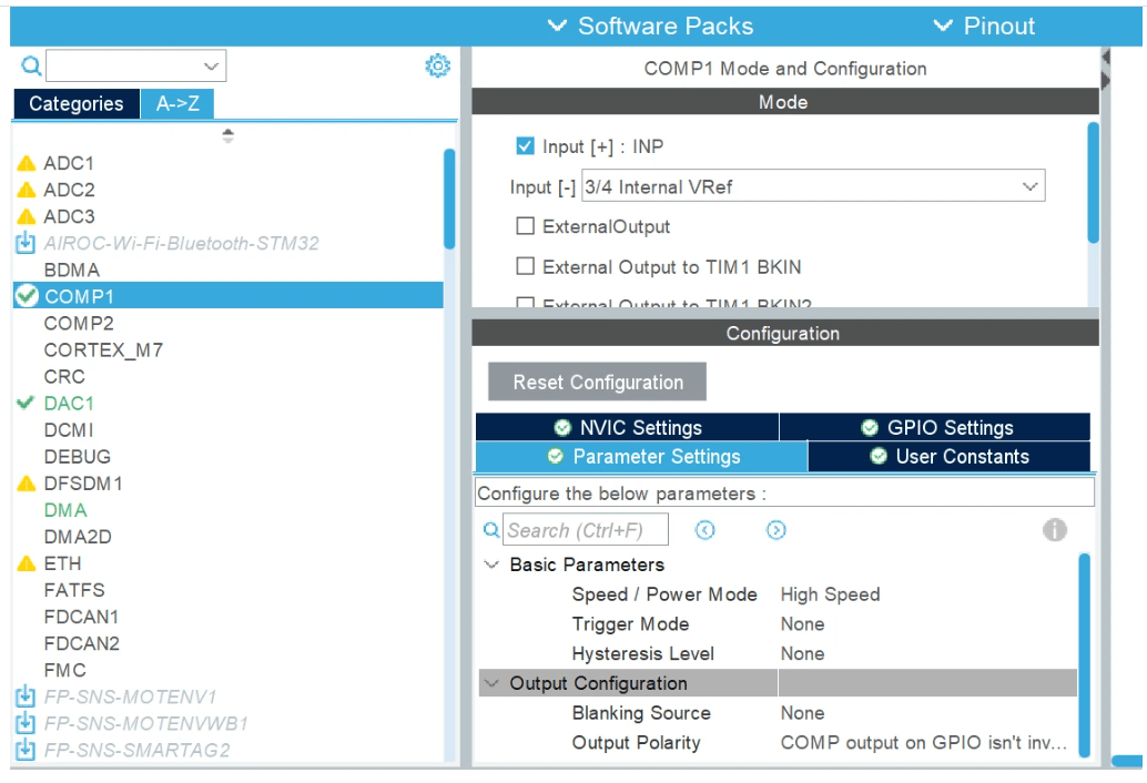
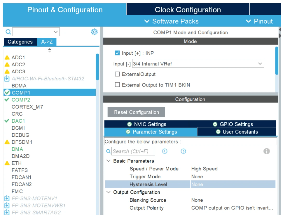
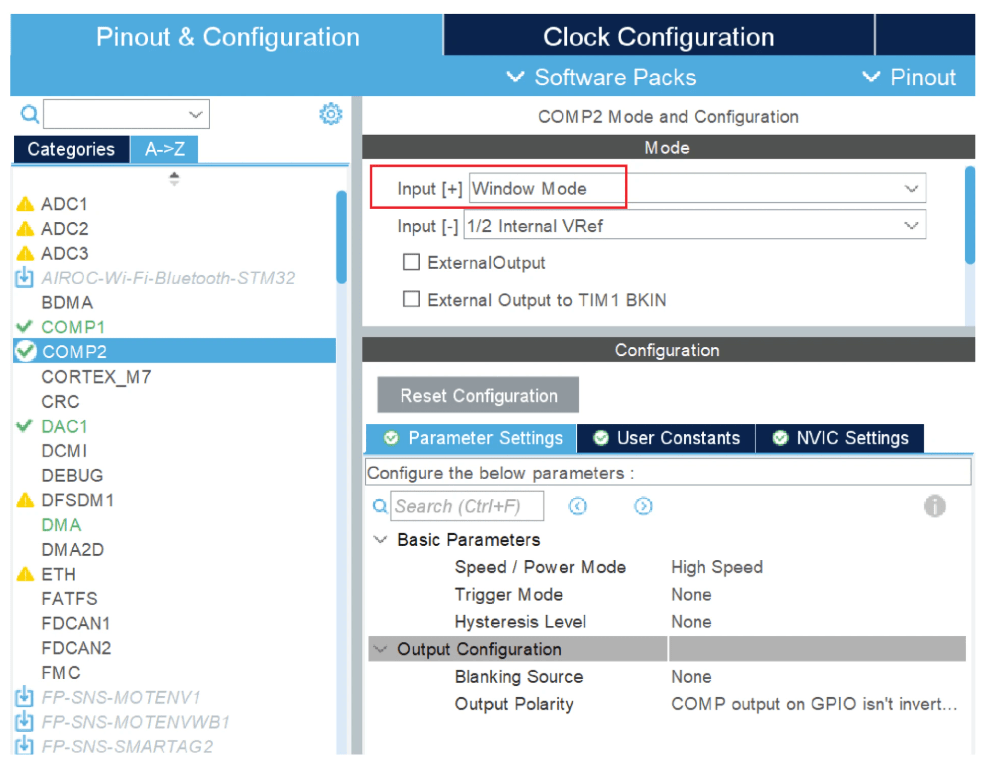
Use STM32CubeMx to specify the mode and required IOC configuration for each comparator.
For example:
1. Open STM32CubeMX.
2. In the left pane, select COMP1.
3. In the right pane, set Input [-], the input voltage (Vin), to 3/4 Internal VRef.
4. In the left pane, select COMP2.
5. In the right pane, set Input [+] to Window Mode and Input [-] to 1/2 Internal VRef.
This example assumes:
Internal Vref as per data sheet is 1.2V
For COMP1, Vref1 = 3/4* (Internal Vref) = 3/4*1.2 = 0.9
For COMP2, Vref2 = 1/2* (Internal Vref) = 1/2*1.2 = 0.6
Input supply voltage considered as per data sheet is 3.3V. In the model we have considered 12-bit DAC, so n=12
V1 = Vref1/Vin (2*n -1) = 0.9/3.3 *4095 = 1117
V2 = Vref2/Vin (2*n -1) = 0.6/3.3 *4095 = 744
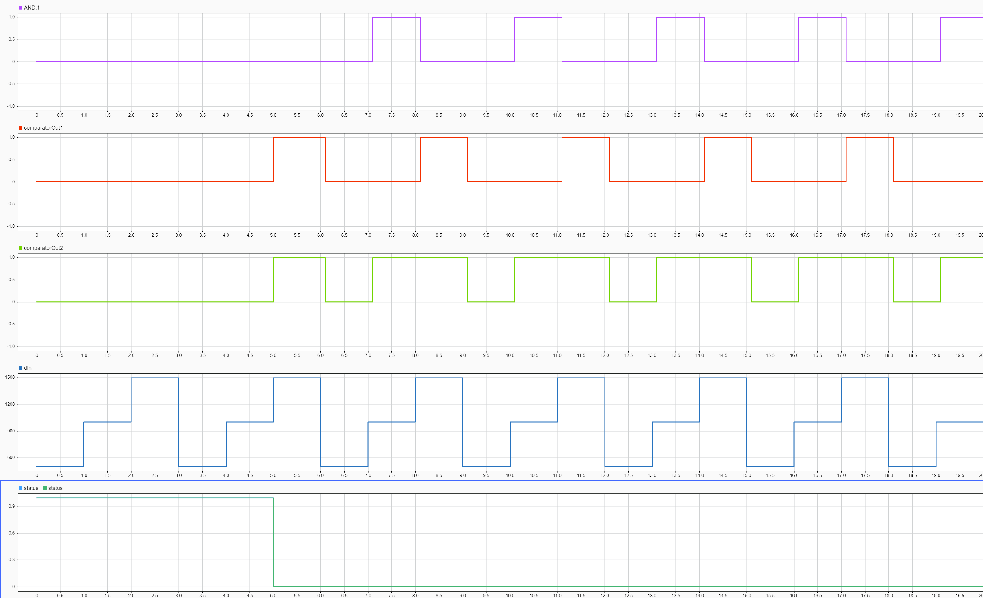
Waveform Analysis
The Simulation Data Inspector displays five waveforms that illustrate the behavior of a three-level stair input sequence processed through a DAC and dual comparators with window detection.
AND:1 (Window Comparison) Waveform - The AND signal (purple waveform at the top of the scope) acts as a window comparator that indicates when the DAC output lies between the two reference thresholds. It remains low (0.0) until the system is enabled at the 5-second mark. Once enabled, it transitions high (1.0) only when dIn is exactly 1000 (higher than the Vref2 threshold of 744 but lower than the Vref1 threshold of 1117). The signal stays low for dIn values of 500 or 1500, effectively highlighting the middle step of the stair sequence.
COMP1 (comparatorOut1) Waveform - The COMP1 signal uses an internal reference threshold of 1117. It remains low (0.0) until the 5-second enable mark. After that point, it transitions high (1.0) only when dIn reaches 1500, and stays low for the 500 and 1000 values.
COMP2 (comparatorOut2) Waveform - The COMP2 signal compares the DAC output against a lower threshold of 744 after the 5-second enable mark. It transitions high (1.0) whenever dIn is 1000 or 1500, and returns to low (0.0) only when the input sequence resets to 500.
dIn (Digital Input) Waveform - The dIn signal follows a repeating stair sequence of 500, 1000, and 1500, with each level held for one second. This three-second cycle provides the digital input values that the DAC converts into analog voltages for evaluation by the comparators.
Status (Step Block) Waveform - The status signal remains high (1.0) for the first five seconds of the simulation, then steps down to low (0.0). This transition at the 5-second mark serves as the enable trigger that activates the comparator outputs.