Design Internally Matched Ultra-Wideband Vivaldi Antenna
This example shows how to model and analyze a vivaldi antenna with an internal matching circuit. The vivaldi is also known as an exponentially tapered slot antenna. The antenna possesses wideband characteristics, low cross polarization and a highly directive pattern. The design is implemented on a single layer dielectric substrate with 2 metal layers; one for a flared slot line, and the feed line with the matching circuit on the other layer. The substrate is chosen as a low cost FR4 material of thickness 0.8 mm. The design is intended for operation over the frequency band 3.1 - 10.6 GHz [1].
Define Antenna Dimensions
The vivaldi antenna is designed to operate between 3 to 11 GHz with dimensions of 45-by-40 mm. At the highest frequency of operation, the structure is approximately -by-. Define the design parameters of the antenna.
Lgnd = 45e-3;
Wgnd = 40e-3;
Ls = 5e-3;
Ltaper = 28.5e-3;
Wtaper = 39.96e-3;
s = 0.4e-3;
d = 5e-3;
Ka = (1/Ltaper)*(log(Wtaper/s)/log(exp(1)));
Create Top Layer Shape
This design consists of three layers. The top layer is the exponentially tapered slot shape, same as the vivaldi antenna in the Slot Antennas. The bottom layer consists of the feed and the matching circuit. The middle layer is the FR4 substrate. The function pcbStack converts any 2-D or 2.5-D antenna from the catalog into a PCB antenna for further modeling and analysis. Create the vivaldi antenna from the catalog and visualize it. Thereafter, move the feed and convert it to the stack representation and access the layer geometry for further modifications.
vivaldiant = vivaldi(TaperLength=Ltaper, ApertureWidth=Wtaper, ...
                      OpeningRate=Ka, SlotLineWidth=s, ...
                      CavityDiameter=d, CavityToTaperSpacing=Ls, ...
                      GroundPlaneLength=Lgnd, GroundPlaneWidth=Wgnd, ...
                      FeedOffset=-10e-3);
figure
show(vivaldiant)

vivaldiant.FeedOffset = -14e-3;
ewant = pcbStack(vivaldiant);
topLayer = ewant.Layers{1};
figure
show(topLayer)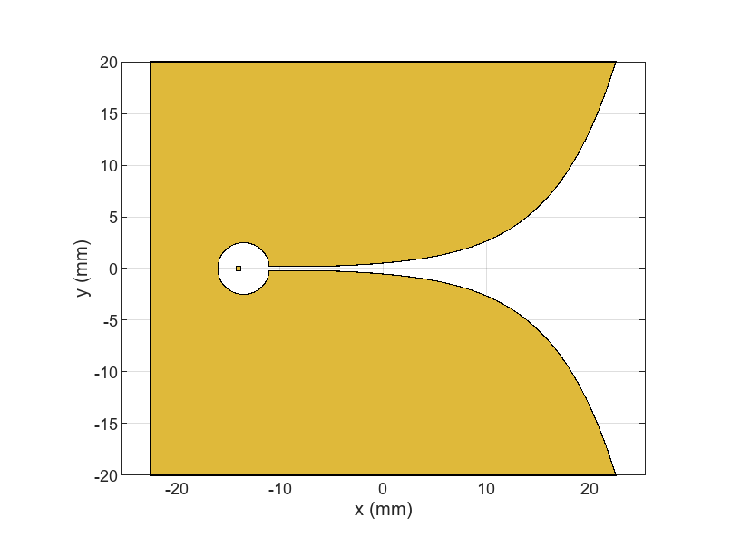
Remove Feed Strip from Vivaldi Structure
The default vivaldi antenna structure in the catalog has an internal feed and the associated feed strip specified at the center of the antenna. This example uses edge feed model. Remove the strip from the vivaldi structure.
cutout = antenna.Rectangle(Length=1e-3, Width=4e-3, Center=[-0.014 0]);
topLayer = topLayer - cutout;
figure
show(topLayer)

Create Matching Circuit for Vivaldi Antenna
Use a stepped microstrip line as a matching circuit with a 90 degree bend terminating into a radial bowtie stub. Use the antenna.Rectangle to create the stepped microstrip line. Perform Boolean addition operation on these shapes to join them.
L1 = 8e-3;
L2 = 4.1e-3;
L3 = 9.1e-3;
W1 = 1.5e-3;
W2 = 1e-3;
W3 = 0.75e-3;
H = 0.8e-3;
fp = 11.2e-3;
th = 90;
patch1 = antenna.Rectangle(Length=L1, Width=W1,...
                            Center=[-(Lgnd/2 - L1/2) -(Wgnd/2 - fp - W1/2)],...
                            NumPoints=[10 2 10 2]);
patch2 = antenna.Rectangle(Length=L2, Width=W2,...
                            Center=[-(Lgnd/2 - L1 - L2/2) -(Wgnd/2 - fp - W1/2)],...
                            NumPoints=[5 2 5 2]);
patch3 = antenna.Rectangle(Length=W3, Width=L3,...
                            Center=[-(Lgnd/2 - L1 - L2 - W3/2) -(Wgnd/2 - fp - W1/2 + W2/2- L3/2)],...
                            NumPoints=[2 10 2 10]);
Create Radial Stub Matching circuit
Use the function makebowtie to create a radial stub matching circuit. It takes inputs for the radius, neck width, flare angle, center, shape of the bowtie, and number of points to create a shape for bowtie.
Bowtie = em.internal.makebowtie(8.55e-3, W3, th, [0 0 0],'rounded',20);
rotatedBowtie = em.internal.rotateshape(Bowtie,[0 0 1],[0 0 0],90);
p = antenna.Polygon(Vertices=rotatedBowtie');

radialStub = translate(p,[-(Lgnd/2 - L1 - L2 - W3/2) -(Wgnd/2 - fp - W1/2 + W2/2- L3) 0]);

bottomLayer = patch1 + patch2 + patch3 + radialStub;
figure
show(bottomLayer)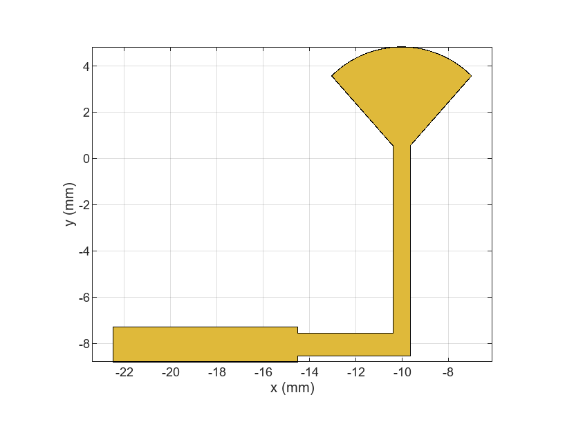
Create PCB Stack
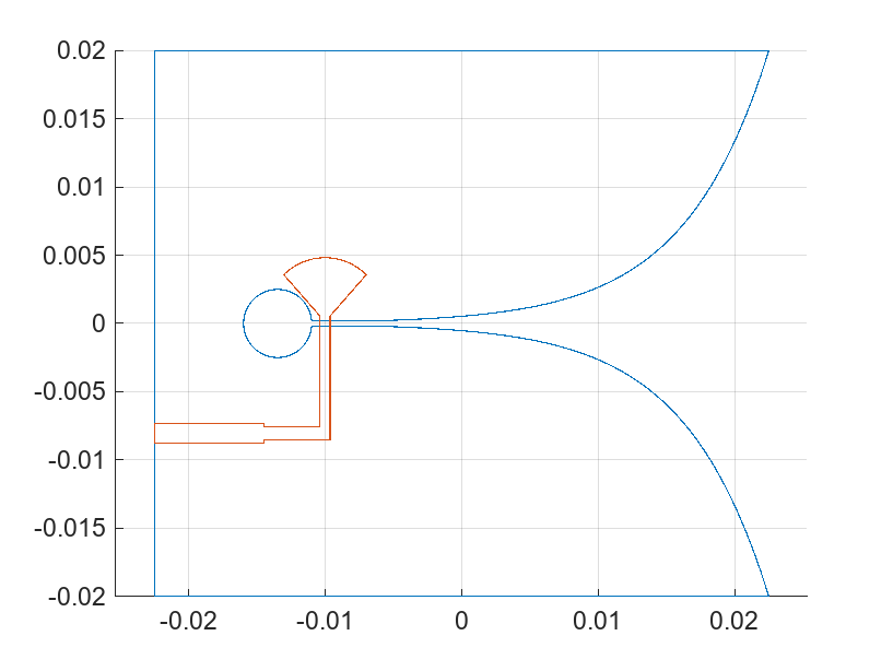
Create the board shape for the antenna. The board is rectangular with size 45 mm-by-40 mm.
boardShape = antenna.Rectangle(Length=Lgnd, Width=Wgnd);
figure
hold on;
plot(topLayer)
plot(bottomLayer)
grid on
Define the Dielectric Substrate
Use an FR4 substrate with relative permittivity of 4.4 and height 0.8 mm for the vivaldi antenna.
substrate = dielectric(Name="FR4", EpsilonR=4.4, Thickness=H);Assign Layers and Define Feed
Assign the layers starting from the top-layer, in this case vivaldi structure, followed by the FR4 dielectric substrate and finally the lowest layer, the matching circuit. The edge-feed is specified between the vivaldi and the matching circuit on the bottom layer. Having the feed line with the matching circuit on the bottom layer reduces any spurious radiation. Define the feed location and the feed diameter as well.
vivaldiNotch = pcbStack;
vivaldiNotch.Name = "vivaldiNotch";
vivaldiNotch.BoardThickness = H;
vivaldiNotch.BoardShape = boardShape;
vivaldiNotch.Layers = {topLayer,substrate,bottomLayer};
vivaldiNotch.FeedLocations = [-(Lgnd/2) -(Wgnd/2 - fp - W1/2) 1 3];
vivaldiNotch.FeedDiameter = W1/2;
figure
show(vivaldiNotch)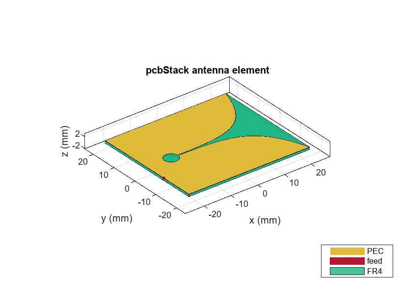
Impedance Analysis
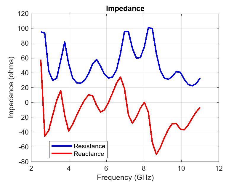
Calculate the antenna impedance over a range of 2.5 GHz to 11 GHz. For the purpose of executing this example, the impedance analysis has been precomputed and saved in a MAT-file. The analysis was performed with the automatic mesh generation mode. Execute the info method on the antenna to get information about the meshing/solution status, analysis frequencies and estimate of the memory required for analysis.
freq = linspace(2.5e9,11e9,41);
bandfreqs = [3.1e9 10.6e9];
freqIndx = nan.*(ones(1,numel(bandfreqs)));
for i = 1:numel(bandfreqs)
    df = abs(freq-bandfreqs(i));
    freqIndx(i) = find(df==min(df));
end
load vivaldi_Notch_auto_mesh
vivaldiInfo = info(vivaldiNotch)
vivaldiInfo = struct with fields:
          IsSolved: "false"
          IsMeshed: "false"
       MeshingMode: "auto"
      HasSubstrate: "true"
           HasLoad: "false"
     PortFrequency: []
    FieldFrequency: []
    MemoryEstimate: []
figure
impedance(vivaldiNotch,freq);
Refine Antenna Mesh
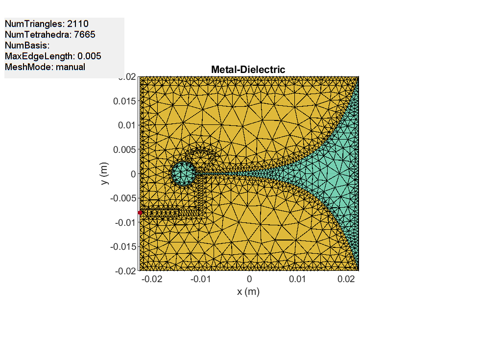
Refine the mesh to check for convergence with the impedance variation over the band. Automatically generated mesh has a 2 cm maximum edge length approximately and a 3 mm minimum edge length. The highest frequency in the analysis range is 11 GHz which corresponds to a 27.3 mm wavelength in the free space. Considering 10 elements per wavelength gives out a 2.7 mm edge length approximately, which is lower than both the maximum and minimum edge length chosen by the automatic mesher. After a few attempts, using a 5 mm maximum edge length and a 0.8 mm minimum edge length resulted in a good solution.
figure
mesh(vivaldiNotch, MaxEdgeLength=5e-3, MinEdgeLength=0.8e-3);
view(0,90)
Due to the size of the mesh, the number of unknowns to obtain an accurate solution increases. As before, the solved structure has been saved to a MAT-file and is loaded here for further analysis.
load vivaldi_Notch_manual_mesh.mat
figure
impedance(vivaldiNotch,freq);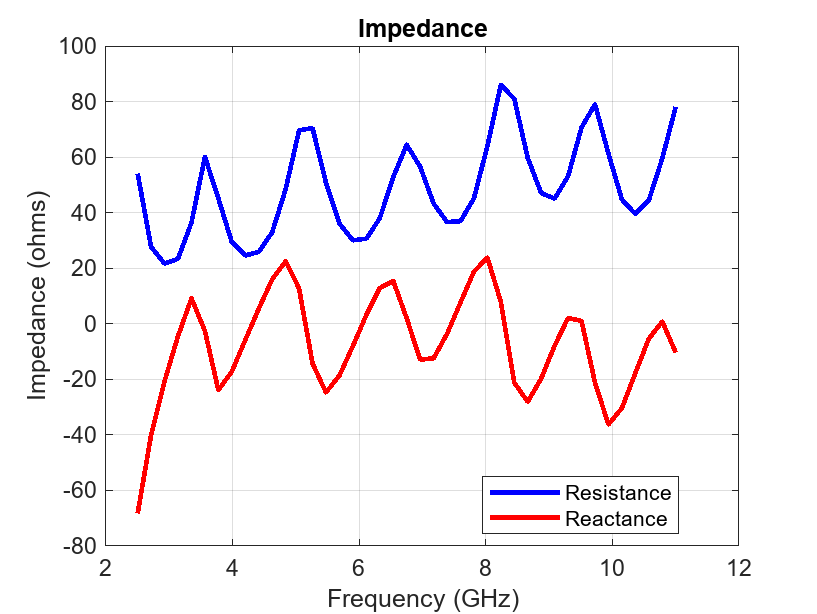
Reflection Coefficient
Calculate the reflection coefficient at the input relative to 50-ohm reference impedance. The reflection coefficient is below -10 dB for the frequency range from 3.1 GHz to 11 GHz. Save the reflection coefficient for use later in calculating the realized gain.
figure
s = sparameters(vivaldiNotch,freq);
rfplot(s);
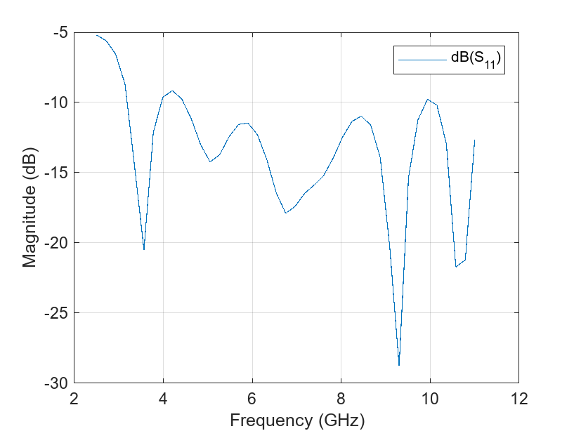
gamma = rfparam(s,1,1);
Realized Gain
The realized gain of antenna includes losses in the dielectric and due to any impedance mismatch. Plot the variation in realized gain with frequency at the antenna boresight at (azimuth,elevation) = (0,0) deg.
G = zeros(1,numel(freq));
az = 0;
el = 0;
for i = 1:numel(freq)
    G(i) = pattern(vivaldiNotch,freq(i),az,el);
end
g = figure;
plot(freq./1e9,G,'-*', LineWidth=2);
xlabel("Frequency (GHz)");
ylabel("Magnitude (dBi)");
grid on;
title("Gain Variation With Frequency");
Compute Mismatch and Calculate Realized Gain
mismatchFactor = 10*log10(1 - abs(gamma).^2);
Gr = mismatchFactor.' + G;
figure(g)
hold on
plot(freq./1e9,Gr,'r-.');
legend("Gain","Realized Gain","Location","best")
title("Gain and Realized Gain Variatin with Frequency")
hold off

The wide impedance bandwidth does not necessarily translate to a wide gain/pattern bandwidth. The highest gain of approximately 9.5 dBi is achieved over the 7 - 10.4 GHz range at boresight. Plot the 3-D pattern in the middle of this sub-band to understand the overall radiation characteristics.
dfsub = abs(freq - (10.4e9+7e9)/2);
subfreqIndx = find(dfsub==min(dfsub));
figure
pattern(vivaldiNotch,freq(subfreqIndx),'Type',"gain");
Phase Center Variation of Antenna
The phase center of an antenna is the local center of curvature of the far-field phase front [2]. It can vary with frequency and observation angle. An analysis of the phase center variation is critical for positioning systems. This is because variations in the phase center directly translate to variations in time delay, which can impact range estimates between a transmitter and a receiver. To understand this, calculate the maximum possible variation in time delay due to a harmonic signal at fmin and another at fmax over a set of observation angles in the far-field. Choose the angles over 2 orthogonal planes; the first specified at elevation = 0 degrees, i.e. the xy-plane and the other at az = 0 degrees, i.e. xz-plane. In the xy-plane use the component of the electric field for analysis while in the xz-plane use the component of the electric field.
Create Points in Far-Field and Calculate Electric Field
Define the far-field sphere radius and the set of observation angles in azimuth and elevation. Choose the two harmonic signal frequencies to be at 3 and 11 GHz respectively.
az = -180:5:180;
el = -90:5:90;
fmin = freq(freqIndx(1));
fmax = freq(freqIndx(2));
R = 100*299792458/fmin;
coord = 'sph';
phi = 0;
theta = 90 - el;
[Points, ~, ~] = em.internal.calcpointsinspace(phi,theta,R,coord);
Calculate Local Phase Variation of E-field
Calculate the electric field at the two frequencies and convert to the spherical component . Since the maximum time delay variation is of interest, first calculate the maximum phase variation between the two frequencies over the set of points in xz-plane.
E_at_fmin = EHfields(vivaldiNotch,fmin,Points);
E_at_fmax = EHfields(vivaldiNotch,fmax,Points);
Eth_at_fmin = helperFieldInSphericalCoordinates(E_at_fmin,phi,theta);
Eth_at_fmax = helperFieldInSphericalCoordinates(E_at_fmax,phi,theta);
phase_at_fmin = angle(Eth_at_fmin);
phase_at_fmax = angle(Eth_at_fmax);
Calculate Time Delay Variation Between the Two Harmonic Signals
delta_phase = max(phase_at_fmin-phase_at_fmax) - min(phase_at_fmin-phase_at_fmax);
delta_omega = 2*pi*(fmax-fmin);
delta_time = pi*delta_phase/180/delta_omega;
delta_timeXZ = delta_time*1e12;
sprintf("The time delay variation in the XZ-plane is: %2.2f %s",delta_timeXZ,'ps')
ans =
"The time delay variation in the XZ-plane is: 2.18 ps"
Repeat the process for the points on the xy-plane and calculate the time delay variation due to the variation.
phi = az;
theta = 0;
delta_omega = 2*pi*(fmax-fmin);
[Points, ~, ~] = em.internal.calcpointsinspace( phi, theta, R,coord);
E_at_fmin = EHfields(vivaldiNotch,fmin,Points);
E_at_fmax = EHfields(vivaldiNotch,fmax,Points);
[~,Ephi_at_fmin] = helperFieldInSphericalCoordinates(E_at_fmin,phi,theta);
[~,Ephi_at_fmax] = helperFieldInSphericalCoordinates(E_at_fmax,phi,theta);
phase_at_fmin = angle(Ephi_at_fmin);
phase_at_fmax = angle(Ephi_at_fmax);
delta_phase = max(phase_at_fmin-phase_at_fmax) - min(phase_at_fmin-phase_at_fmax);
delta_time = pi*delta_phase/180/delta_omega;
delta_timeXY = delta_time*1e12;
sprintf("The time delay variation in the XY-plane is: %2.2f %s",delta_timeXY,'ps')
ans =
"The time delay variation in the XY-plane is: 2.75 ps"
Observation
The time delay variation in the two planes that bisect the antenna boresight, reveal that the phase center is relatively stable. The average time delay variation of approximately 2 ps translates to a maximum range error of less than 1 mm.
Generate Gerber Files for Prototyping
The vivaldi antenna can be fabricated by using the gerber file generation capability in the toolbox. For this example, a SMA Edge connector from Amphenol[3] was chosen and Advanced Circuits[4] was used as the manufacturing service. In addition, on the PCBWriter object, the layer of solder mask was not enabled. The fabricated antenna, is shown below.
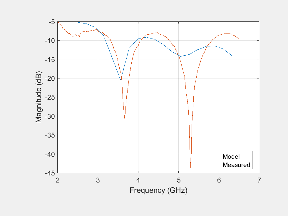
Performance in the 3-6 GHz Range
The fabricated antenna was tested using a desktop network analyzer. Since the upper limit of the analyzer was 6.5 GHz, the results of the fabricated antenna were compared with the analysis from the model.
fLim = 6.5e9;
findx = find(freq>fLim);
freq2 = freq(1:findx(1)-1);
s_model = sparameters(vivaldiNotch, freq2);
rfplot(s_model);
s_proto = sparameters('UWB2.s1p');
hold on
rfplot(s_proto)
legend("Model","Measured","Location","best")
Conclusion
The proposed antenna covers the Federal Communications Commission defined UWB spectrum and has more than 3.5:1 impedance bandwidth (from 3 GHz to more than 11 GHz). The antenna realized gain achieved over the band 3-10 GHz at boresight is very close to the gain result. Comparing the reflection coefficient in 3 - 6 GHz range of the fabricated prototype and the model reveals an acceptable performance. The reflection coefficient between 4-4.75 GHz does degrade to about -8 dB.
Reference
[1] High Gain Vivaldi Antenna for Radar and Microwave Imaging Applications International Journal of Signal Processing Systems Vol. 3, No. 1, June 2015 G. K. Pandey, H. S. Singh, P. K. Bharti, A. Pandey, and M. K. Meshram.
[2] Vishwanath Iyer, Andrew Cavanaugh, Sergey Makarov, R. J. Duckworth,'Self-Supporting Coaxial Antenna with an Integrated Balun and a Linear Array Thereof', Proceedings of the Antenna Application Symposium, Allerton Park, Monticello, IL, pp.282-284, Sep. 21-23rd 2010.
[3] “Product Data Drawing - SMA Jack End Launch Receptacle.” Accessed August 8, 2023. https://www.mouser.com/datasheet/2/18/2985-6037.PDD_0-918701.pdf
[4] “Printed Circuit Board Manufacturer - PCB Manufacturing and Assembly.” Accessed August 8, 2023. https://www.4pcb.com/.
See Also
You can also select a web site from the following list:
Americas
- América Latina (Español)
- Canada (English)
- United States (English)
Europe
- Belgium (English)
- Denmark (English)
- Deutschland (Deutsch)
- España (Español)
- Finland (English)
- France (Français)
- Ireland (English)
- Italia (Italiano)
- Luxembourg (English)
- Netherlands (English)
- Norway (English)
- Österreich (Deutsch)
- Portugal (English)
- Sweden (English)
- Switzerland
- United Kingdom (English)