Generate FIFO Interface DPI Component for UART Receiver
This example shows the full workflow of how to generate a SystemVerilog DPI component for a FIFO buffer interface meant to be integrated with a UART receiver. The interface is written in MATLAB®, and exported to an HDL simulator. The SystemVerilog files for the UART receiver and its testbench are also provided.
For demonstrative purposes, this example uses ModelSim™ 10.3c in 64-bit Windows® 7. However, this same procedure can be easily replicated for other systems and simulators.
Requirements and Prerequisites
Third-party products required for this example:
Simulators: Siemens® ModelSim/QuestaSim™ or Cadence® Xcelium™
One of the supported C compilers: Microsoft® Visual C++, or GNU GCC
Background
A universal asynchronous receiver and transmitter (UART) is a circuit that sends and receives data through a serial line. UART's are usually used with the RS-232 standard and contain a receiver and transmitter. However in this example only a receiver is used.
The serial transmission starts with a 'start bit' which is 0, followed by data bits, and ends with a 'parity bit' and a 'stop bit'. Transmission of a single byte is show in the following figure:

The transfer is asynchronous, which means that there is no clock information, therefore the receiver and transmitter must agree on what baud rate, stop bits, and parity bit are used. In this example one byte will be transferred with a baud rate of 19,200, 1 stop bit and no parity bits.
An oversampling scheme will be used to estimate the middle point of the data bit at a rate 16 times the baud rate, as shown in the figure below.

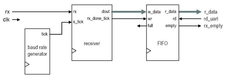
The following schematic illustrates the UART receiver design.

Step 1: MATLAB Design
The first step is to write the MATLAB code that will satisfy the requirements of your design, you should try to capture the requirements in a testbench. In this example our design consists of a first in first out (FIFO) buffer of 8 words.
Design: FIFO_Buffer
Testbench: FIFO_Buffer_tb
Step 2: Make sure the MATLAB testbench captures the requirements
Run the testbench to make sure there are no runtime errors, the figure below should be plotted.
FIFO_Buffer_tb

Note that the testbench is exercising the design in the following way:
Clock cycles<15: Write 6 bytes (write signal enabled, read signal disabled), then Read the 6 bytes (read signal enabled,write signal disabled).
Clock cycles>15: Read and write simultaneously. (For example: The byte that is written is read in the next clock cycle.)
Step 3: Generate the DPI component and verify the behavior in the HDL Simulator
To generate the component execute the following command:
dpigen -testbench FIFO_Buffer_tb FIFO_Buffer -args {0,int8(0),0}
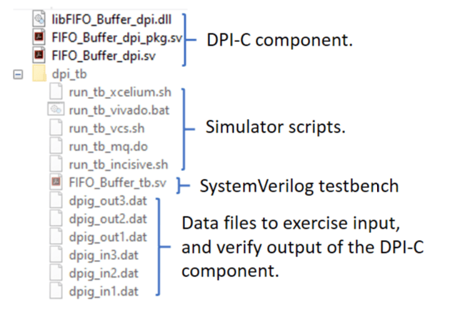
The figure below shows the relevant files for this example.

Once DPIGEN generates the DPI component and its testbench you can run the SystemVerilog testbench by following the steps below:
Start ModelSim/QuestaSim in GUI mode.
Change your current directory to
codegen/dll/FIFO_Buffer/dpi_tbunder the code generation directory in your HDL simulator.Enter the following command to start your simulation
do run_tb_mq.do
The following wave forms will be generated:

Note that this matches our MATLAB testbench where we write 6 bytes and then read them, followed by simultaneously writing and reading 8 bytes.
When the simulation finishes, you should see the following text printed in your console:
**************TEST COMPLETED (PASSED)**************
Step 4: Integrate the Generated DPI Component into the UART Receiver design
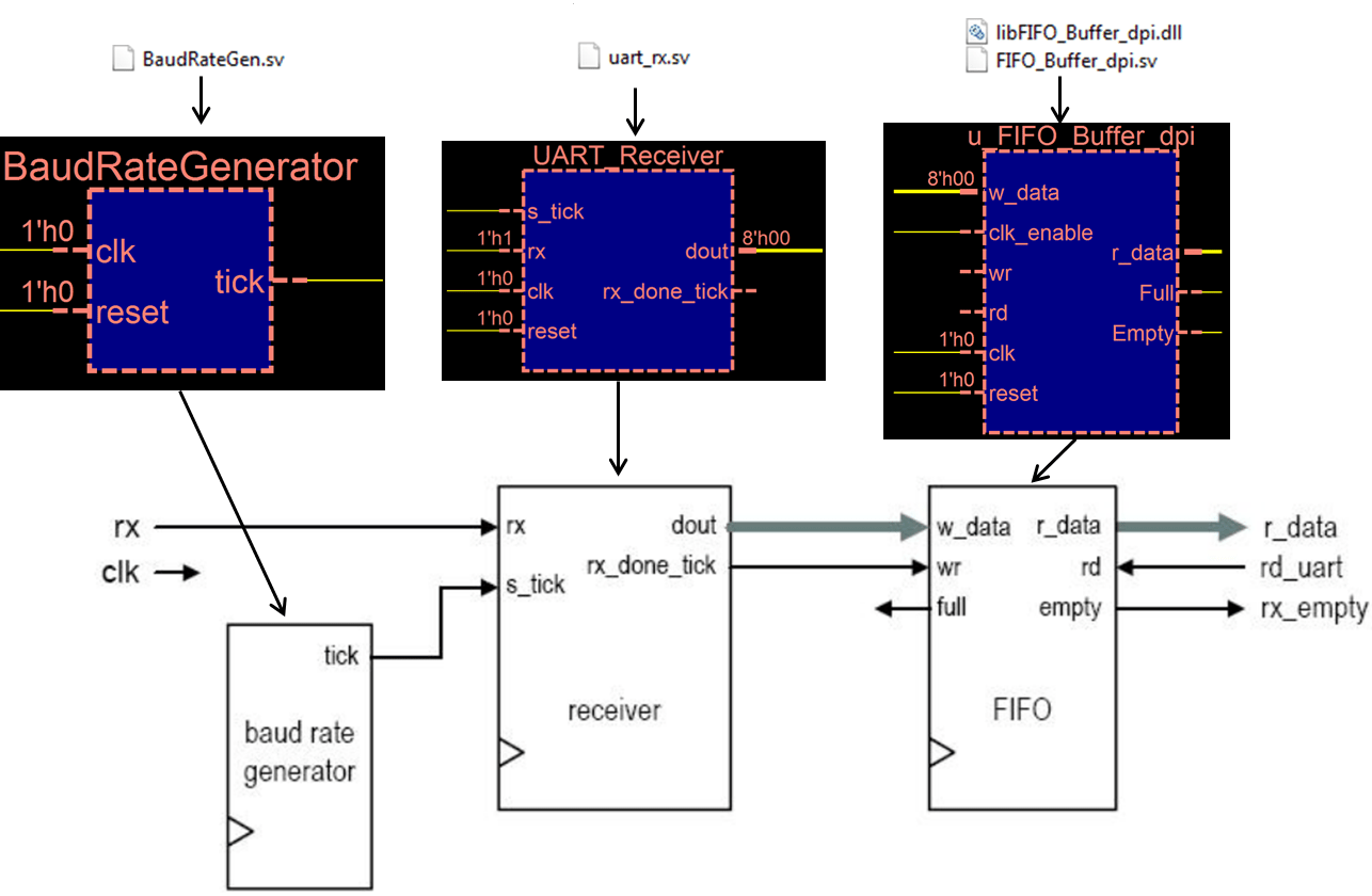
After the DPI component behavior has been verified, it is time to integrate it into the UART receiver. The following figure shows the files required for the different components.

To exercise the UART receiver with the DPI component integrated, the testbench named 'uart_rx_FIFO_tb.sv' has been provided. The UART component is instantiated in the testbench as shown below:
// Instantiate DUT generated using MATLAB Based SystemVerilog DPI
FIFO_Buffer_dpi u_FIFO_Buffer_dpi(
.clk(clk),
.clk_enable(clk_enable),
.reset(reset),
.wr(rx_done_tick),
.w_data(dout),
.rd(rd),
.Empty(Empty),
.r_data(r_data),
.Full(Full)
);
Step 5: Simulate UART Receiver
To simulate the design successfully, make sure the following files are in the same folder:

Similar to step 3, open Modelsim and run the .do file using:
do run_tb.do
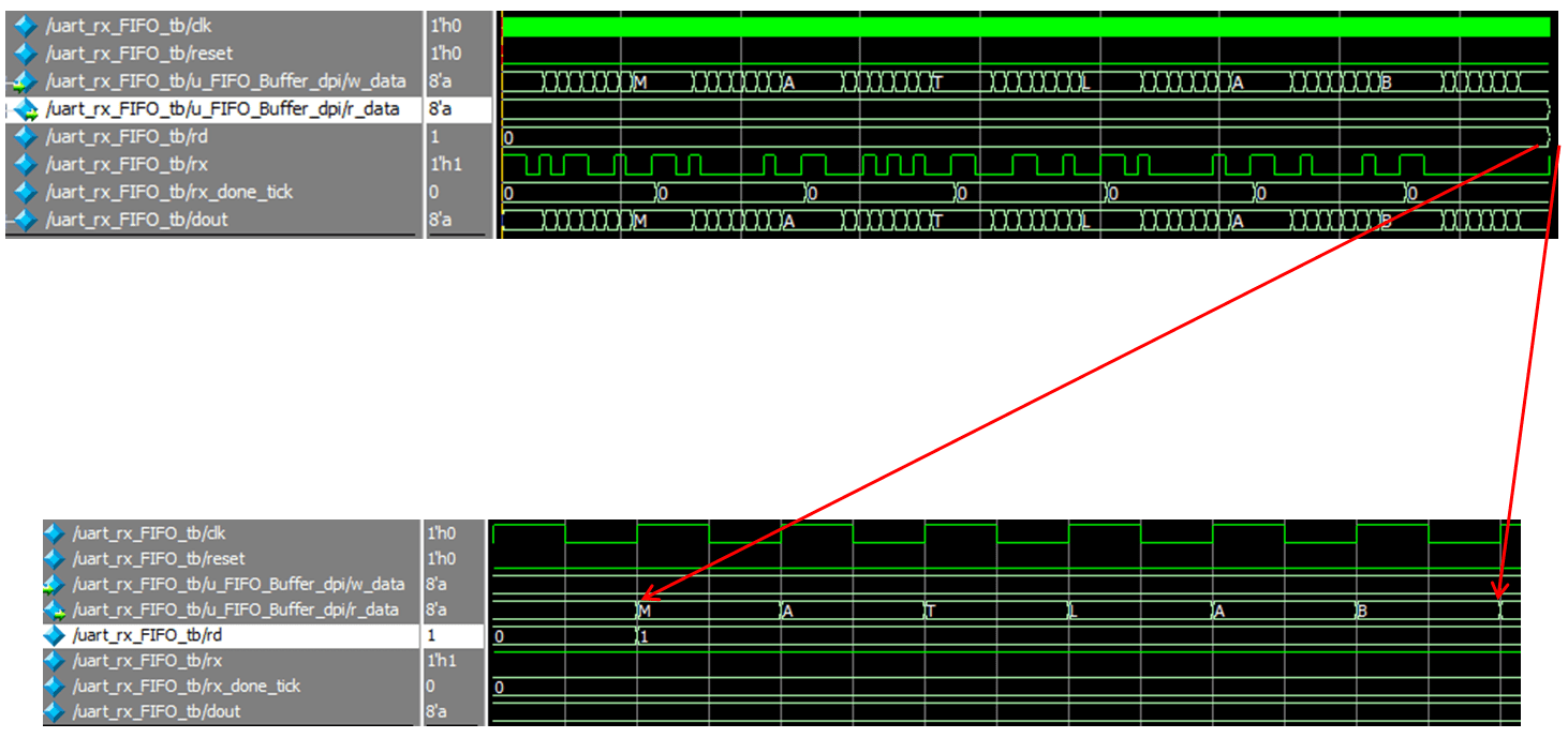
The following wave forms are generated:

In the testbench 6 ASCII letters ('MATLAB') are transferred via the serial 'rx' signal, and written into the FIFO buffer. After the 6th letter transfer is complete the 'rd' signal is asserted to get the letters ('MATLAB') back in 'r_data'.
References
Pong P. Chu (2008), FPGA Prototyping by Verilog Examples. Hoboken, New
Jersey: John Wiley & Sons, Inc.