pcb2D
Description
Use pcb2D to create a 2-D cross section model of a transmission
line for use with the 2-D solver.
Creation
Description
pcb2d = pcb2D returns a default 2-D cross section of a
microstripline represented by two metal layers with a Teflon substrate in
between.
pcb2d = pcb2D( sets
Properties of a 2-D cross
section of a microstripline using one or more name-value arguments. Properties not
specified retain their default values. PropertyName=Value)
S = sparamaters(pcb2d,freq,LineLength=0.5) calculates the s
parameters of 2D cross section of microstripline at a specified frequency and line
length.
Properties
Object Functions
show | Display PCB component structure or PCB shape |
sparameters | Calculate S-parameters for RF PCB objects |
rlgc | Compute resistances, inductances, conductances, and capacitances |
propagationDelay | Compute propagation delay of transmission line |
getZOdd | Calculate odd mode impedance of differential PCB transmission line |
getZEven | Calculate even mode impedance of differential PCB transmission line |
Examples
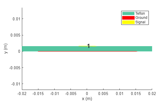
Create a 2-D cross section object with a board width of 0.04 meters.
pcb2d = pcb2D(BoardWidth=0.04)
pcb2d =
  pcb2D with properties:

           Name: 'MyPCB2D'
     BoardWidth: 0.0400
    BoardCenter: 0
         Layers: {[1×1 trace2D]  [1×1 dielectric]  [1×1 trace2D]}
show(pcb2d)
Calculate s parameters of cross section at 1.9 GHz.
S = sparameters(pcb2d,1.9e9)
S =
  sparameters with properties:

      Impedance: 50
       NumPorts: 2
     Parameters: [2×2 double]
    Frequencies: 1.9000e+09
Version History
Introduced in R2026a