Analyzing Crosstalk Between PCB Traces
This example shows how to create a pair of close traces using traceLine object and performs analysis on those traces to calculate the amount of unwanted coupling to the passive trace.
Create Traces
trace1 = traceLine;
trace1.Length = [10 5*sqrt(2) 10 5*sqrt(2) 10]*1e-3;
trace1.Angle  = [0 45 0 -45 0];
trace1.Width  = 3e-3;
trace1.Corner = "Miter";
trace2 = copy(trace1);
trace2.Length = [11 6*sqrt(2) 6 6*sqrt(2) 11]*1e-3;
trace2 = translate(trace2, [0,-5e-3,0]);
trace = trace1 + trace2 ;
figure
show(trace);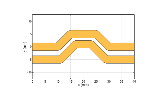
Create PCB Component
Use the pcbComponent to create the PCB stack for the shape. For creating a PCB stack, the trace created above is used as a top layer. The middle layer is a dielectric and the bottom layer is a ground plane. Use the dielectric object to create the Teflon dielectric. Use traceRectangular object to create a rectangular ground plane. Assign the trace, dielectric(d), and groundplane to the Layers property of the pcbComponent. Assign the FeedLocations at the ends of the trace and visualize it.
pcb = pcbComponent;
d = dielectric("Teflon");
d.Thickness = pcb.BoardThickness;
groundplane = traceRectangular(Length=40e-3,Width=40e-3,Center=[40e-3/2,0]);
pcb.Layers = {trace,d,groundplane};
pcb.FeedLocations = [0,0,1,3;40e-3,0,1,3;40e-3,-5e-3,1,3;0e-3,-5e-3,1,3];
pcb.BoardShape = groundplane;
pcb.FeedDiameter = trace1.Width/2;
figure
show(pcb);
Use current function to plot the current distribution on the trace
figure
current(pcb,1e9,scale="log");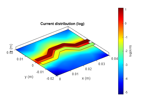
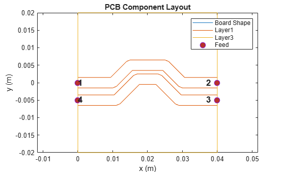
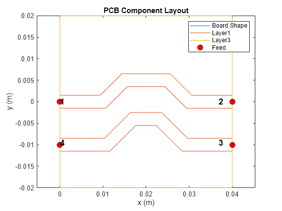
Use the layout function to show the layout of the pcbComponent.
figure
layout(pcb);
Use sparameters function to calculate the leakage power from Trace 1 to Trace 2.
spar = sparameters(pcb,linspace(0.1e9,10e9,51));
figure
rfplot(spar,2:4,1)
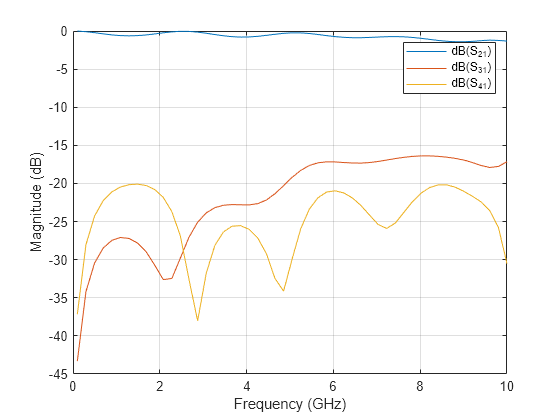
The S31 shows the power coupled from the top trace to the bottom trace. This is the unwanted coupling from the top line to the bottom line and must be reduced. To reduce the coupling, increase the spacing between the traces.
Increase the Spacing Between Traces
trace1 = traceLine;
trace1.Length = [10 5*sqrt(2) 10 5*sqrt(2) 10]*1e-3;
trace1.Angle  = [0 45 0 -45 0];
trace1.Width  = 3e-3;
trace1.Corner = "Sharp";
trace2 = copy(trace1);
trace2.Length = [11 6*sqrt(2) 6 6*sqrt(2) 11]*1e-3;
trace2 = translate(trace2, [0,-10e-3,0]);
trace = trace1 + trace2 ;
figure
show(trace);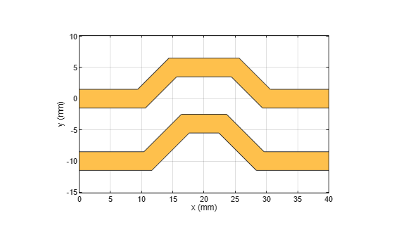
Create PCB Component
Update the properties of the created earlier and visualize it.
groundplane = traceRectangular(Length=40e-3,Width=40e-3,Center=[40e-3/2,0]);
pcb.Layers = {trace,d,groundplane};
pcb.FeedLocations = [0,0,1,3;40e-3,0,1,3;40e-3,-10e-3,1,3;0e-3,-10e-3,1,3];
figure
show(pcb);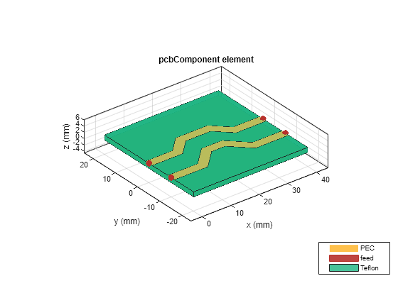
Use current function to plot the current distribution on the trace.
figure
current(pcb,1e9,scale="log");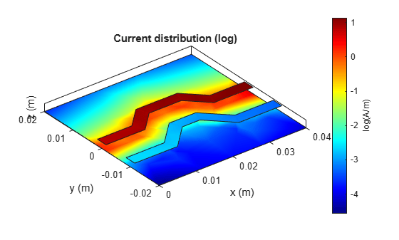
Use the layout function to show the layout of the pcbComponent.
figure
layout(pcb);
Use sparameters function to calculate the leakage power from Trace 1 to Trace 2.
spar = sparameters(pcb,linspace(0.1e9,10e9,101));
figure
rfplot(spar,2:4,1)
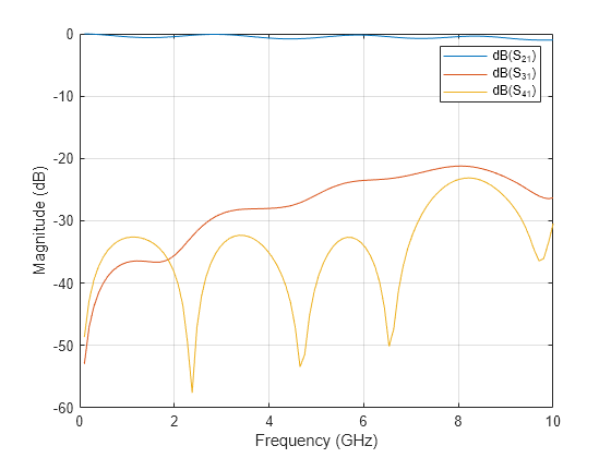
When the spacing between the traces is doubled to 10 mm, the coupling also reduces by around 10 dB and reaches to less than -25 dB.
Plot the Crosstalk Induced Voltage
Define a pulse signal with rise time and fall time and use the timeresp function to plot the output signal at port 2 for the input pulse signal.
sampleTime = 1e-9;
t = (0:999)'*sampleTime;
input = [0.05*(0:20)';ones(1,78)'; 0.05*(20:-1:0)'; zeros(1,80)'];
input = repmat(input,5,1);
fit   = rationalfit(spar,3,1,NPoles=128);
output = timeresp(fit,input,sampleTime);
figure
yyaxis left;
plot(t,input);
yyaxis right;
plot(t,output);
title("Crosstalk between the Traces");
xlabel("Time (sec)");
ylabel("Voltage (volts)");
legend("Vinput","Output",Location="SouthWest");
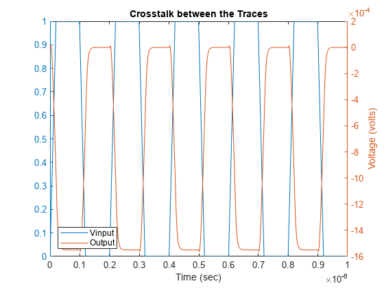
The output signal magnitude is around 0.1 mV as seen from the result.
References
1) https://incompliancemag.com/visualizing-crosstalk-in-pcbs/
2) Basic Principles of Signal Integrity, Altera