Create and Analyse Dual Characteristics of Complementary Split Ring Resonators from Gerber Files
This example shows how to create a complementary split ring resonator (CSRR) from Gerber files and subsequently analyze the model. The Gerber file format is used in printed circuit board (PCB) manufacturing and is available in two formats: RS-274D, which was the initial release standard, and RS-274X, which is the newer extended Gerber format. The RF-PCB Toolbox™ supports the newer RS-274X format both to generate Gerber files from a PCB model and to create the PCB model from a set of Gerber files.
The CSRRs have been proposed for the synthesis of metamaterials. The basic unit cell that exhibits negative permittivity is imported using the gerber files in the first section, which shows band stop response at 0.9 GHz, and later the left-handed (LH) behavior of the metamaterial is achieved which exhibits pass band at the same frequency by creating the slit on the top layer of the transmission line and the same is analyzed [1].
This example shows how to model the above-described PCB structure from the gerber file.
Introduction
A set of Gerber files includes information about layer geometry, layer mask, solder paste usage on the layers, drill file and so on. To create a PCB model out of these files, you need layer files that specify the PCB geometry, and if available a drill file to specify any plated through-hole (PTH) vias. The geometry of the layers is specified through either a top and a bottom layer file, with extensions .gtl and .gbl, or a Gerber file, with the extension .gbr. The RF-PCB Toolbox supports the Excelling format to specify drill information with file extensions .txt or .drl.
The complimentary metamaterial resonator structure contains three layers on which the top layer is the transmission line in microstrip form and the bottom layer is the CSRR. The CSRR model is created from the gerber file in first section. Later, a gap capacitor is introduced by modifying the top layer of CSRR in second section and further, their behaviors are analyzed in the third section .
Import Top and Bottom Layer from Gerber file
The first step is to import a top-layer and bottom-layer Gerber file from the workspace using the gerberRead function. This will create a PCBReader object. The PCBReader object provides access to the stack up that holds the information of the metal and dielectric layers and also any drill files that describe a PTH via from one metal layer to another if available.
The CSRR model imported using StackUp method contains three layers corresponding to the model of CSSR and returns the model with additional two layers of air dielectric as the first and last layer by default.
Import the top and bottom layers from the gerber file by passing .gtl and .gbl file as inputs to the function gerberRead and use stack up method to create the layers.
P1 = gerberRead('CSRRWOSlit.gtl','CSRRWOSlit.gbl');
P1.StackUp;
Pass the created PCB reader object as input to pcbComponent and clean up the layer vertices by rounding it off up to some tolerance. Here 6 is picked as the tolerance as the layer dimensions are in mm units. Later, view the top and bottom layer of the structure to measure its feed width and board dimensions.
The imported PCBReader object contains five layers, where layer2 and layer4 holds the top and bottom layer of the CSRR structure.
pb = pcbComponent(P1);

pb.Layers{2}.Vertices =  round(pb.Layers{2}.Vertices,6);
pb.Layers{4}.Vertices =  round(pb.Layers{4}.Vertices,6);

% Visualize the top and bottom layer of the PCB structure
figure;
show(pb.Layers{2});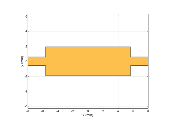
figure;
show(pb.Layers{4});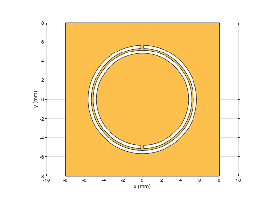
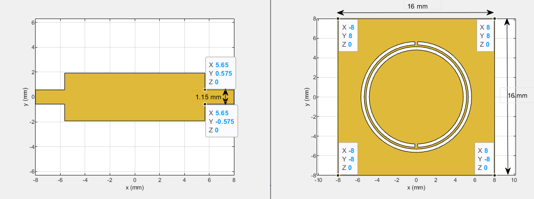
The pointers are placed to measure the dimensions of Feed Width and the board shape as shown above. It is observed that, the Feed Width is 1.15 mm and ground plane length and width are 16 mm each.
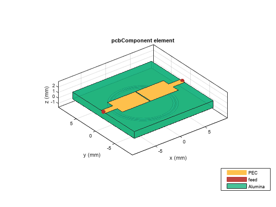
Next step is to modify the layers of pcb object. Set the PCB Board dimensions, feed diameter and feed location from the measured values accordingly and visualize the PCB model.
%Define substrate
h   = 1.27e-3;
sub = dielectric('Name',{'Alumina'},'EpsilonR',10.2,'LossTangent',0.0023,'Thickness',h);

% Define Board thickness
pb.BoardThickness = h;

% Define pcb Layers
pb.Layers = {pb.Layers{2},sub,pb.Layers{4}};

% Define Board Shape
gndL = 16e-3;
gndW = 16e-3;
gnd  = antenna.Rectangle('Length',gndL,'Width',gndW);
pb.BoardShape = gnd;

% Define Feed Diameter and set Feed location from the measured values
Fw = 1.15e-3;
pb.FeedDiameter = Fw/2;
pb.FeedViaModel = 'strip';
pb.FeedLocations =  [-gndL/2,0,1,3;gndL/2,0,1,3];

% Visualize pcb Component (pb)
figure;
show(pb)

Create Slit Model of CSRR
Create the slit complimentary split ring resonator by introducing the slit in the microstrip line which exhibits gap capacitor due to which the structure can show its characteristics as LH Metamaterial.
Modify the top layer from the pcbComponent object (pb) by introducing the slit in the top layer of CSSR structure and visualize it.
pbs = copy(pb);
g = 0.15e-3;
W = 3.85e-3;
% Create the rectangle to introduce the gap
trace = traceRectangular('Length',g,'Width',W,'Center',[0,0]);
toplayer = pbs.Layers{1};
% Substract the rectangle from the top layer
slit  = toplayer-trace;
% Reassign the top layer
pbs.Layers{1} = slit;
% Visualize pcb Component (pbs)
figure;
show(pbs)
Analyze Above CSRR Model With and Without Slit
The CSRR model shown without slit (pb) and with slit (pbs) on the top layer is analyzed in the frequency range of 0.1 GHz to 2 GHz using the sparameters method to compute the transmission co-efficient and is plotted using the rfplot method.
% Analyse sparameters of CSRR without slit
spar = sparameters(pb,linspace(0.1e9,2e9,51));
figure;
rfplot(spar,2,1);
% Analyse sparameters of CSRR with slit
spar = sparameters(pbs,linspace(0.1e9,2e9,31));
hold on;
rfplot(spar,2,1)
title('Transmission Co-efficient of CSRR models');
legend('S21 without slit','S21 with slit');
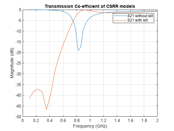
It is observed from the above graph that the transmission coefficient S21 for the CSRR metamaterial of negative permittivity lines exhibits the band stop response at resonant frequency of 0.9 GHz, and the Left-handed behavior which is achieved by introducing gap capacitors in microstrip line exhibits the band pass response at the same frequency.
Conclusion
The microstrip lines loaded with CSRRs has been analyzed in two different forms on the same substrate and is observed that they exhibit stop and pass band at same desired frequency.
The gerberRead function is used to import the gerber files of CSRR. One can create, a PCBReader object, and subsequently use that object to generate the PCB model using a pcbComponent object.
Reference
Jordi Bonache, Marta Gil*, Ignacio Gil, Joan García, and* Ferran Martín*, “On the Electrical Characteristics of Complementary Metamaterial Resonators,” IEEE MICROWAVE AND WIRELESS COMPONENTS LETTERS, VOL. 16, NO. 10, OCTOBER 2006.*