DDR5 SDRAM Transmitter/Receiver IBIS-AMI Model
This example shows how to create generic DDR5 transmitter and receiver IBIS-AMI models using the library blocks in SerDes Toolbox™ and have been Verified by Intel®. Since DDR5 DQ signals are bidirectional, this example creates Tx and Rx models for the SDRAM. The generated models conform to the IBIS-AMI specification.
DDR5 SDRAM Tx/Rx IBIS-AMI Model Setup in SerDes Designer App
The first part of this example sets up and explores the target transmitter and receiver architectures using the blocks required for DDR5 in the SerDes Designer app. The SerDes system is then exported to Simulink® for further customization and IBIS-AMI model generation.
Type the following command in the MATLAB® command window to open the ddr5_sdram model:
>> serdesDesigner('ddr5_sdram')

The SDRAM has a DDR5 transmitter (Tx) using no equalization. The SDRAM also has a DDR5 receiver (Rx) using a variable gain amplifier (VGA) with 7 pre-defined settings and a 4-tap decision feedback equalizer (DFE) with built-in clock data recovery.
Configuration Setup
Symbol Time is set to
208.3ps, since the target operating rate is4.8Gbps for DDR5-4800.Target BER is set to
100e-18.Signaling is set to
Single-ended.Samples per Symbol and Modulation are kept at default values, which are
16andNRZ(nonreturn to zero), respectively.
Transmitter Model Setup
The DDR5 SDRAM has no transmit equalization, so only an analog model is required.
The Tx AnalogOut model is set up so that Voltage is
1.1V, Rise time is100ps, R (output resistance) is48 ohms, and C (capacitance) is0.65pF. The actual analog models used in the final model will be generated later in this example.
Channel Model Setup
Channel loss is set to
5dB, which is typical of DDR channels.Single-ended impedance is set to
40ohms.Target Frequency is set to
2.4GHz, which is the Nyquist frequency for 4.8 GHz
Receiver Model Setup
The Rx AnalogIn model is set up so that R (input resistance) is
40ohms and C (capacitance) is0.65pF. The actual analog models used in the final model will be generated later in this example.The VGA block is set up with a Gain of 1 and the Mode set to
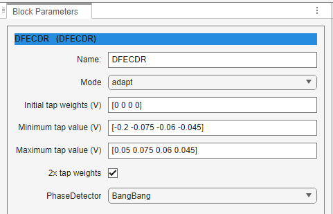
off. Specific VGA presets will be added later in this example after the model is exported to Simulink.The DFECDR block is set up for four DFE taps by including four Initial tap weights set to 0. The Minimum tap value is set to
[-0.2 -0.075 -0.06 -0.045]V, and the Maximum tap value is set to[0.05 0.075 0.06 0.045]V. The PhaseDetector is set toBangBang.Note: the DFECDR offers an option for "2X Taps." Check this option to have pulse response values match convention used by JEDEC. Uncheck this option to use pulse response values directly from the plot. If unsure, leave this option checked for consistency with the JEDEC specification.
Plot Statistical Results
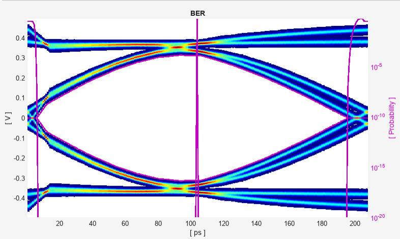
Use the SerDes Designer Add Plots button to visualize the results of the DDR5 SDRAM setup.
Add the BER plot from Add Plots and observe the results.
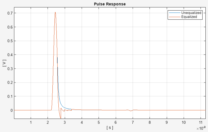
Add the Pulse Response plot from Add Plots and zoom into the pulse area to observe the results.
Export SerDes System to Simulink
Click Save and then click on the Export button to export the configuration to Simulink for further customization and generation of the AMI model executables.
DDR5 SDRAM Tx/Rx IBIS-AMI Model Setup in Simulink
The second part of this example takes the SerDes system exported by the SerDes Designer app and customizes it as required for DDR5 in Simulink.
Review the Simulink Model Setup
The SerDes System imported into Simulink consists of Configuration, Stimulus, Tx, Analog Channel and Rx blocks. All the settings from the SerDes Designer app have been transferred to the Simulink model. Save the model and review each block setup.

Double-click the Configuration block to open the Block Parameters dialog box. The parameter values for Symbol time, Samples per symbol, Target BER, Modulation and Signaling are carried over from the SerDes Designer app.
Double-click the Stimulus block to open the Block Parameters dialog box. You can set the waveform creation method and the number of symbols to simulate. This block is not carried over from the SerDes Designer app.
Double-click the Tx block to look inside the Tx subsystem. Since there is no algorithmic model for the transmitter, the Tx subsystem is simply a pass through from the WaveIn to WaveOut ports.
Double-click the Analog Channel block to open the Block Parameters dialog box. The parameter values for Target frequency, Loss, Impedance and Tx/Rx Analog Model parameters are carried over from the SerDes Designer app.
Double-click on the Rx block to look inside the Rx subsystem. The subsystem has the VGA and DFECDR blocks carried over from the SerDes Designer app. An Init block is also introduced to model the statistical portion of the AMI model.
Run the Model
Run the model to simulate the SerDes system.
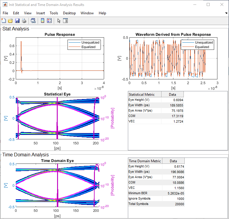
Two plots are generated. The first is a live time domain (GetWave) eye diagram that is updated as the model is running.
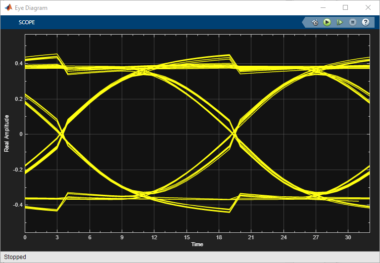
After the simulation has completed the second plot contains views of the Statistical (Init) and Time Domain (GetWave) results, along with reported Eye metrics for each.
Review Rx VGA Block
Inside the Rx subsystem, double-click the VGA block to open the VGA Block Parameters dialog box.
The Mode and Gain settings are carried over from the SerDes Designer app.
Update Rx DFECDR Block
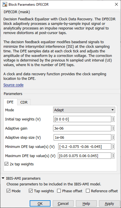
Inside the Rx subsystem, double-click the DFECDR block to open the DFECDR Block Parameters dialog box.
The Initial tap weights, Minimum DFE tap value, and Maximum tap value RMS settings are carried over from the SerDes Designer app. The Adaptive gain and Adaptive step size are set to
3e-06and1e-06, respectively, which are reasonable values based on DDR5 SDRAM expectations.Expand the IBIS-AMI parameters to show the list of parameters to be included in the IBIS-AMI model.
Deselect Phase offset and Reference offset to remove these parameters from the AMI file, effectively hard-coding these parameters to their current values.
Generate DDR5 SDRAM IBIS-AMI Models
The final part of this example takes the customized Simulink model, modifies the AMI parameters for a DDR5 SDRAM, and then generates IBIS-AMI compliant DDR5 SDRAM model executables, IBIS and AMI files.
Open the Block Parameter dialog box for the Configuration block and click on the Open SerDes IBIS-AMI Manager button. In the IBIS tab inside the SerDes IBIS-AMI manager dialog box, the analog model values are converted to standard IBIS parameters that can be used by any industry-standard simulator.
Review Transmitter (Tx) AMI Parameters
Open the AMI-Tx tab in the SerDes IBIS-AMI manager dialog box. Notice that there are no model-specific parameters since the DDR5 SDRAM Tx does not have any equalization.
Add Tx Jitter Parameters
To add Jitter parameters for the Tx model click the Reserved Parameters... button to bring up the Tx Add/Remove dialog, then select the Tx_Dj and Tx_Rj boxes and click OK to add these parameters to the Reserved Parameters section of the Tx AMI file. The following values allow you to fine-tune the jitter values to meet DDR5 jitter mask requirements.
Note: All JEDEC DDR5 SDRAM values are currently available for DDR5-4800.
Set Tx Deterministic Jitter Value
Select Tx_Dj, then click the Edit... button to bring up the Add/Edit AMI Parameter dialog.
Verify the Type is set to
UI.Verify the Format is set to
Value.Set the Current Value to
0.1000Click OK to save the changes.
Set Tx Random Jitter Value
Select Tx_Rj, then click the Edit... button to bring up the Add/Edit AMI Parameter dialog.
Verify the Type is set to
UI.Verify the Format is set to
Value.Set the Current Value to
0.0050Click OK to save the changes.
Update Receiver (Rx) AMI Parameters
Open the AMI-Rx tab in the SerDes IBIS-AMI manager dialog box. The reserved parameters are listed first followed by the model-specific parameters adhering to the format of a typical AMI file.
Set the VGA Gain:
Highlight Gain.
Click the Edit… button to launch the Add/Edit AMI Parameter dialog box.
In the Description box, type
Rx Amplifier Gain.Make sure Format is set to List, then set Default to
1.In the List values box, enter
[0.5 0.631 0.794 1 1.259 1.585 2]In the List_Tip values box, enter
["-6 dB" "-4 dB" "-2 dB" "0 dB" "2 dB" "4 dB" "6 dB"]Click OK to save the changes.
Set First DFE Tap Weight
Highlight TapWeight 1.
Click the Edit… button to launch the Add/Edit AMI Parameter dialog box.
Make sure Format is set to Range and set Typ =
0, Min =-0.2, and Max =0.05.Click OK.
Set Second DFE Tap Weight
Highlight TapWeight 2.
Click the Edit… button to launch the Add/Edit AMI Parameter dialog box.
Make sure Format is set to Range and set Typ =
0, Min =-0.075, and Max =0.075Click OK.
Set Third DFE Tap Weight
Highlight TapWeight 3.
Click the Edit… button to launch the Add/Edit AMI Parameter dialog box.
Make sure Format is set to Range and set Typ =
0, Min =-0.06, and Max =0.06Click OK.
Set Fourth DFE Tap Weight
Highlight TapWeight 4.
Click the Edit… button to launch the Add/Edit AMI Parameter dialog box.
Make sure Format is set to Range and set Typ =
0, Min =-0.045, and Max =0.045Click OK.
Add Rx Jitter Parameters
To add Jitter parameters for the Rx model click the Reserved Parameters... button to bring up the Rx Add/Remove dialog, then select the Rx_Rj, Rx_Dj and Rx_Receiver_Sensitivity boxes and click OK to add these parameters to the Reserved Parameters section of the Rx AMI file. The following values allow you to fine-tune the jitter values to meet DDR5 jitter mask requirements.
Note: All JEDEC DDR5 SDRAM values are currently available for DDR5-4800.
Set Rx Random Jitter Value
Select Rx_Rj, then click the Edit... button to bring up the Add/Edit AMI Parameter dialog.
Verify the Type is set to
UI.Verify the Format is set to
Value.Set the Current Value to
0.00375Click OK to save the changes.
Set Rx Deterministic Jitter Value
Select Rx_Dj, then click the Edit... button to bring up the Add/Edit AMI Parameter dialog.
Verify the Type is set to
UI.Verify the Format is set to
Value.Set the Current Value to
0.01750Click OK to save the changes.
Set Rx Receiver Sensitivity Value
Select Rx_Receiver_Sensitivity, then click the Edit... button to bring up the Add/Edit AMI Parameter dialog.
Verify the Format is set to
Value.Set the Current Value to
0.040Click OK to save the changes.
Export Models
Open the Export tab in the SerDes IBIS-AMI manager dialog box.
Update the Tx model name to
ddr5_sdram_tx.Update the Rx model name to
ddr5_sdram_rx.Note that Tx and Rx corner percentage is set to
10. This scales the minimum/maximum analog model corner values by +/-10%.Verify that Dual model is selected for both the Tx and the Rx AMI model settings. This creates model executables that support both statistical (Init) analysis and time-domain (GetWave) simulation.
Set the Rx model Bits to ignore value to
250000to allow sufficient time for the Rx DFE taps to settle during time domain simulations.Set the Models to export to Both Tx and Rx and ensure that all files have been selected to be generated (IBIS file, AMI file(s) and DLL file(s)). Note that while the Tx does not implement any equalization, we are still generating a pass-through model that will allow Tx jitter to be added to the simulation if desired.
Set the IBIS file name to
temp_ddr5_sdram.ibsClick the Export button to generate models in the Target directory.
Note: If additional Simulink simulations are run, the Rx Bits to Ignore value will need to be set a value less than the Number of symbols set in the Stimulus block dialog in order for the time domain results to be output.
Update DDR5 Analog Models
To accommodate different topologies, loading configurations, data rates and transfers, DDR5 requires variable output drive strength and input on-die termination (ODT). While the same algorithmic AMI model is used, multiple analog models are required to cover all these use cases. The generation of these analog models is out of scope for this example, so a completed IBS file with the following analog models in it is available in the current example directory:
POD11_IO_ZO34_ODTOFF: 34 ohm output impedance with no input ODT.
POD11_IO_ZO48_ODTOFF: 48 ohm output impedance with no input ODT.
POD11_IN_ODT34_C: Input with 34 ohm ODT.
POD11_IN_ODT40_C: Input with 40 ohm ODT.
POD11_IN_ODT48_C: Input with 48 ohm ODT.
POD11_IN_ODT60_C: Input with 60 ohm ODT.
POD11_IN_ODT80_C: Input with 80 ohm ODT.
POD11_IN_ODT120_C: Input with 120 ohm ODT.
POD11_IN_ODT240_C: Input with 240 ohm ODT.
To generate this complete IBIS file, the following changes were made to temp_ddr5_sdram.ibs using a text editor:
Created one pin with a signal_name of DQ1_sdram and model_name of dq.
Added two drivers with Model_type of I/O and named them POD11_IO_Z034_ODTOFF and POD11_IO_Z048_ODTOFF, respectively.
Added seven receiver models and named them:
a) POD11_IN_ODT34_C
b) POD11_IN_ODT40_C
c) POD11_IN_ODT48_C
d) POD11_IN_ODT60_C
e) POD11_IN_ODT80_C
f) POD11_IN_ODT120_C
g) POD11_IN_ODT240_C
Added VI curves and Algorithmic Model sections to all above mentioned models.
Added a Model Selector section that references all above mentioned models.
Test Generated IBIS-AMI Models
The DDR5 transmitter and receiver IBIS-AMI models are now complete and ready to be tested in any industry-standard AMI model simulator.
References
[1] IBIS 7.0 Specification, https://ibis.org/ver7.0/ver7_0.pdf.
See Also
VGA | DFECDR | SerDes Designer