DDR5 Implementation Kit
Implement a 1-slot generic DDR5 RDIMM interface for pre-layout analysis or post-layout verification.
DDR5 is an industry standard dynamic memory format operating at a maximum of 6400M transfers per second. The standard is defined by JEDEC in the DDR5 JEDEC Specification JESD79-5.
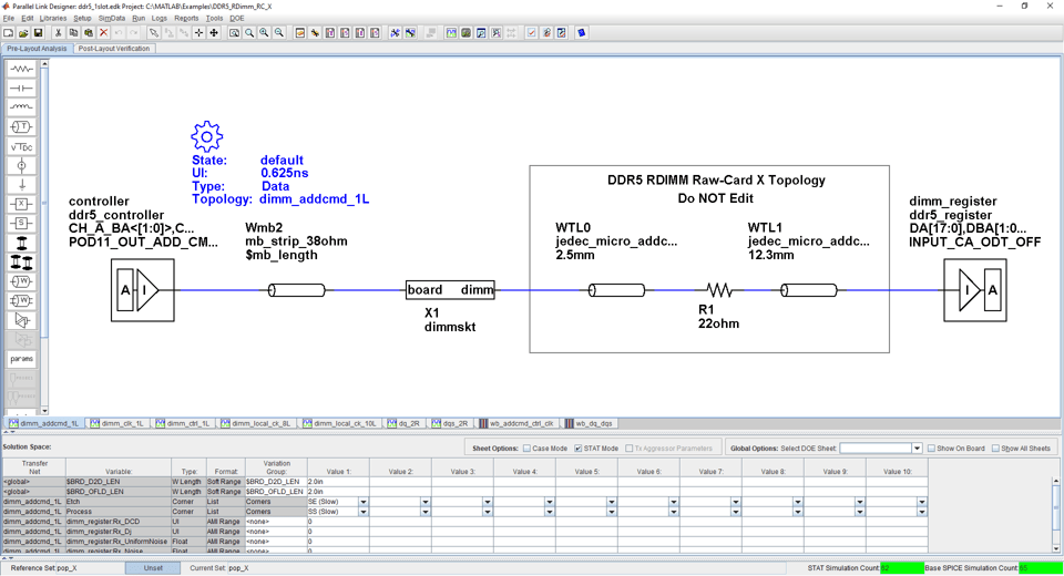
This DDR5 implementation signal integrity kit includes all the transfer nets, waveform processing levels and simulation models for a 1-slot generic DDR5 RDIMM interface. This includes buffer models for a generic DDR5 controller, register and SDRAM, along with complete waveform processing levels. You can modify the kit to match your exact DDR5 implementation. Then, perform complete pre-layout solution space analysis and/or full post-layout verification for waveform quality and timing margins.
Open 1-Slot DDR5 Kit
Open the 1-slot DDR5 kit in the Parallel Link Designer app using the openSignalIntegrityKit function.
openSignalIntegrityKit("DDR5_RDimm_RC_X");

Kit Overview
Project name: DDR5_RDimm_RC_X
Interface name: ddr5_1slot
Two independent DDR5 channels in the generic controller: DDR5_0 and DDR5_1
72-bits per channel (64 data, 8 ECC)
288-pin buffered DDR5 RDIMM
Address/Command 1N timing utilized (can be set up for 2N if desired)
Data mask (DM) not used
The slot is populated with Raw Card “X” DDR5 Registered DIMM modules. Raw Card X used for setup and is not a JEDEC specified Raw Card.
Number of SDRAMs: 18
Package Type: Planar, 78 ball FPGA
Number of Ranks: 2
Width: x4
This kit supports both HSPICE and IsSpice4 simulators. No specific version of either simulator is required when running this kit.
For more information about the generic DDR5 using a mock Raw Card X RDIMM implementation signal integrity kit, including block diagrams, system configurations, transfer nets and libraries, refer to the document DDR5_RDimm_RC_X.pdf that is attached to this example as a supporting file.
References
[1] JEDEC: DDR5 SDRAM. JESD79-5, July 2020.