Parallel Link Design
The Parallel Link Designer app provides a dedicated system-level design and analysis environment for parallel links. Capture your parallel link designs graphically and experiment with different physical layouts and parameter sweeping to determine setup/hold timing and voltage margins for high-speed parallel links. Analyze parallel interfaces for compliance with timing and signal integrity constraints.
Use the Parallel Link Designer app to configure parallel links. Set simulation parameters, specify corner conditions, and define stimulus patterns. Set up pre-layout analysis to run SPICE and to conduct waveform and timing data analysis to analyze your custom parallel links. View and interpret the results using the Signal Integrity Viewer app. You can also set up and analyze the post-layout PCB database of your parallel link design if you have a license for RF PCB Toolbox™. You can modify the stackup and padstack models and customize vias and see how the changes impact your design.
Categories
- Parallel Link Design Concepts
Learn the basics of parallel link design projects using the Parallel Link Designer app
- Configure Parallel Link Projects
Configure parallel link projects for simulations
- Pre-Layout Analysis of Parallel Link Projects
Analyze parallel link projects before designing board layouts
- Post-Layout Verification of Parallel Link Projects
Verify the layout design of your system against design guidelines or specification rules
- Scripting in Parallel Link Projects
Use MATLAB scripting commands to control the Parallel Link Designer app
- Visualize and Interpret Parallel Link Project Analysis Results
Visualize and interpret the network characterization and statistical and time domain analysis results
Featured Examples
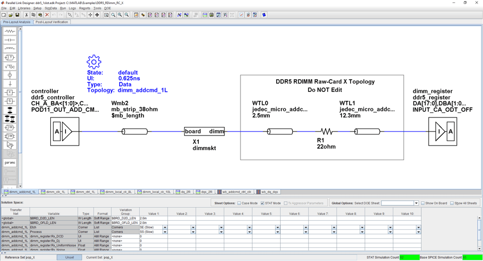
DDR5 Implementation Kit
Implement a 1-slot generic DDR5 RDIMM interface for pre-layout analysis or post-layout verification.
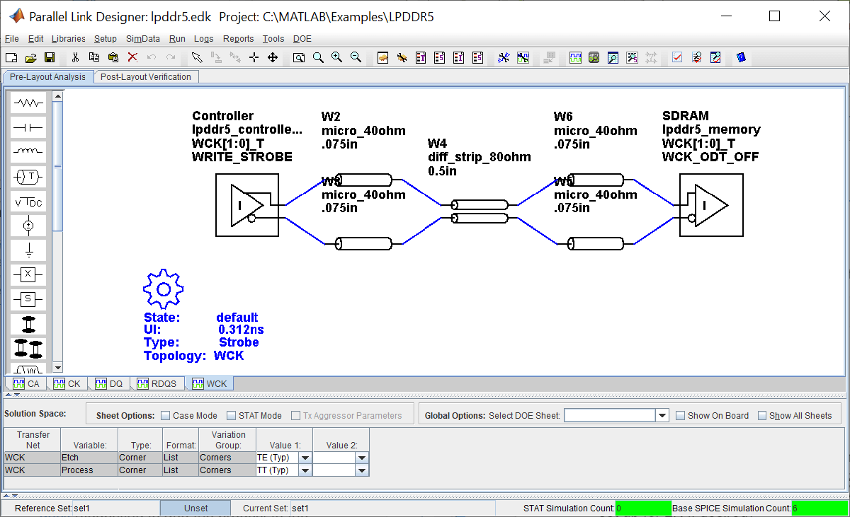
Low-Power DDR5 Architectural Kit
Implement a low-power DDR5 (LPDDR5) interface for pre-layout analysis or post-layout verification.
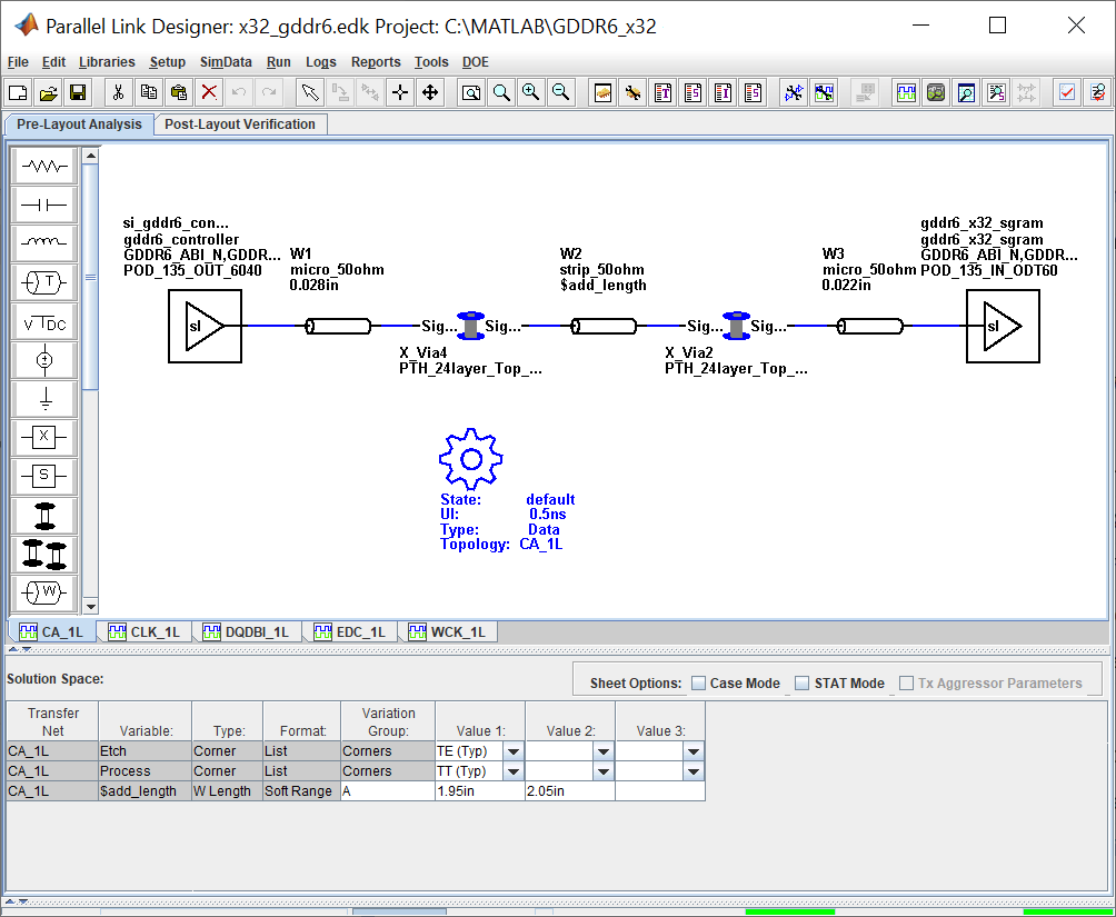
GDDR6 x32 Architectural Kit
Implement a 32-bit GDDR6 interface for pre-layout analysis or post-layout verification.
DDRx Timing and Waveform Mask Analysis
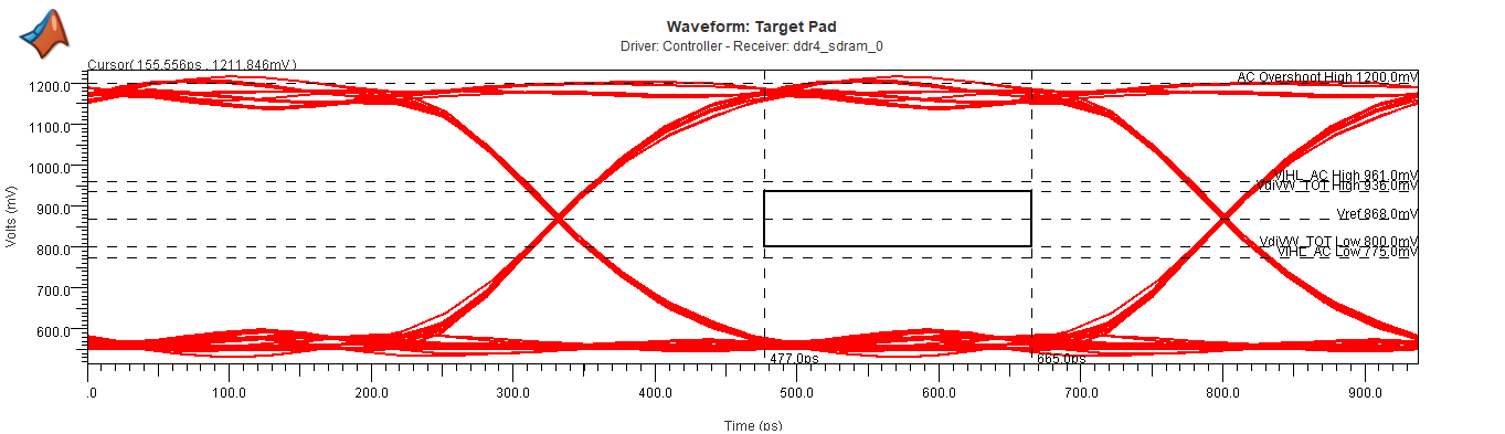
Use the Parallel Link Designer app to perform timing analysis for the DDR (Double Data Rate) family of memory interface protocols. You can use either Setup and Hold margins or by waveform eye-diagram compliance masks to perform the timing analysis. The DDR Memory Down (DDR4_MD) example kit uses both timing and waveform mask analysis. Specifically for DDR4 systems, timing analysis is performed on clock-address/command interface, and waveform compliance masks are applied to strobe-data(DQS-DQ) interface. Other DDR types may use only timing analysis, or only waveform mask analysis or a blend depending on individual standards.
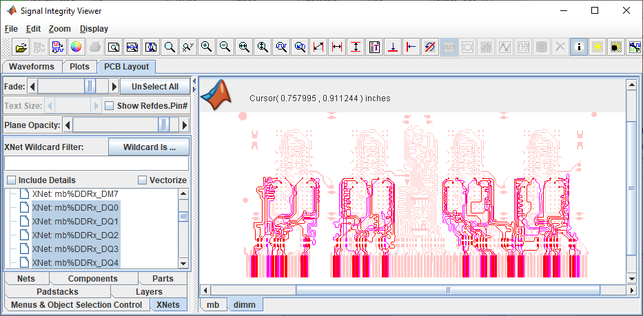
Post-Layout Analysis of DDRx Interface with CPU and DIMMs
Show how to use the Parallel Link Designer app to set up a post-layout analysis of a DDRx interface on a Main Board, which has a CPU connected to two DIMM slots, to verify that waveform quality and timing margins are met by the PCB database. Most of the steps illustrated in this example are also applicable to Serial Link Designer for post-layout analysis of SerDes links.
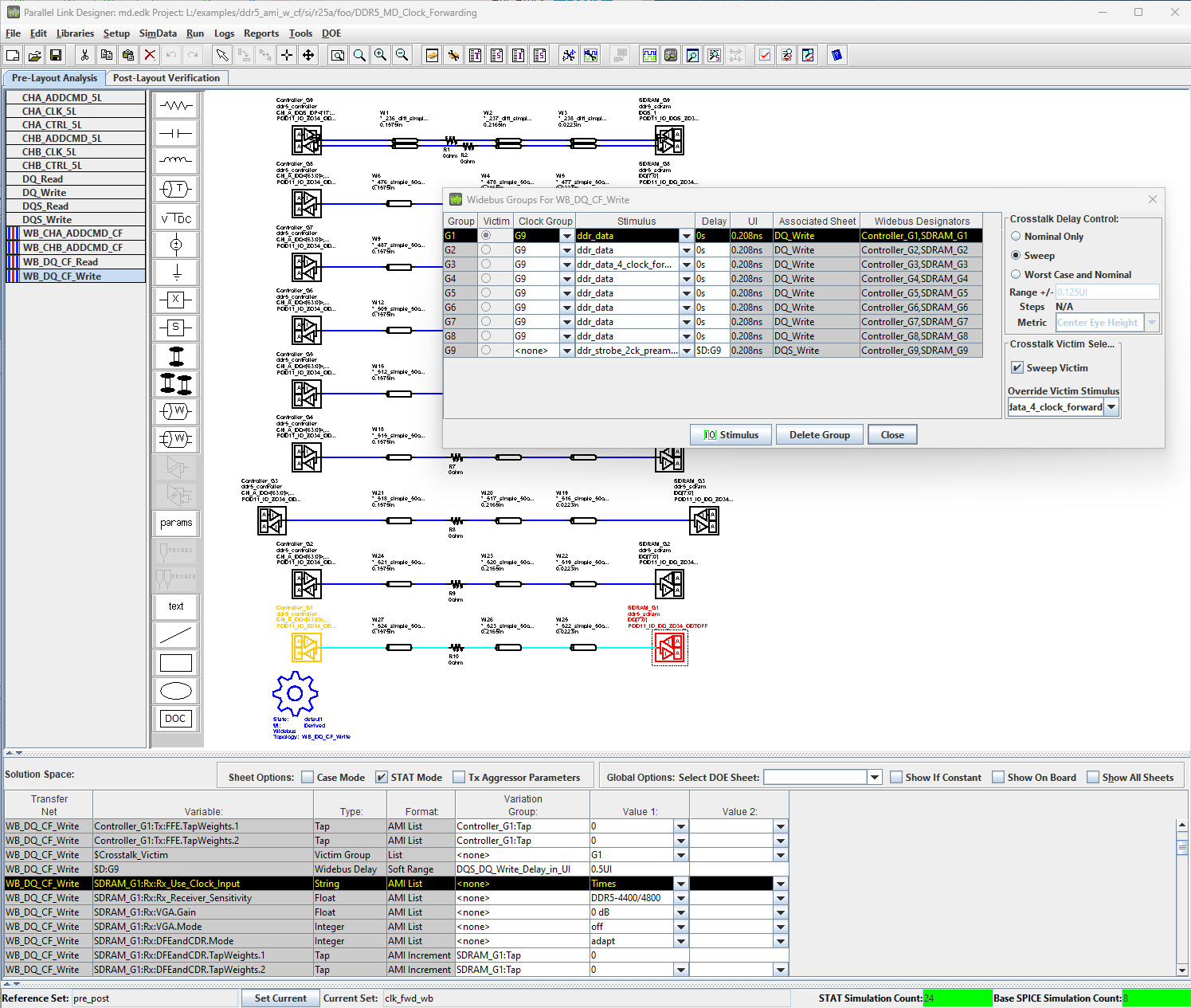
DDR5 IBIS-AMI with Clock Forwarding
Use Signal Integrity Toolbox™ for MATLAB® to analyze a DDR5 interface with the IBIS-AMI feature Clock-Forwarding enabled for analysis of system margins. IBIS BIRD 204, "DQ_DQS GetWave Flow for Clock Forwarding Modeling," added the ability to pass in an external Clock signal (or Strobe, as appropriate) to an Address (or Data) IBIS-AMI receiver GetWave model using the clock_times pointer defined by the IBIS specification. A new AMI Reserver Parameter, Rx_Use_Clock_Input, is used to enable this functionality. This BIRD has been officially accepted and is now part of the IBIS 7.1 specification.