Simultaneous Bi-Directional Analysis in Simulink
R2026bThis example shows how to model and simulate simultaneous bi-directional (SBD) die-to-die links using the SerDes Toolbox. It explains how static replica and adaptive echo-cancellation approaches map to the IBIS-AMI framework. The model contains a far-end transmitter, an interposer channel, and a local transmitter and receiver. The example compares the eye before replica subtraction, after replica subtraction, and after adaptive cancellation. It then illustrates the process to export compiled IBIS-AMI models for IP-protected distribution and integrate the result with Parallel Link Designer for system-level analysis.
This example uses SerDes Toolbox, Signal Integrity Toolbox, and RF Toolbox. It also demonstrates functionality from the Statistics and Machine Learning Toolbox.
Motivation and Background
Modern computing workloads—AI training, high-performance computing, and large-scale data centers—demand ever-increasing bandwidth, yet single-chip scaling is approaching fundamental physical limits. As transistor scaling yields diminishing returns, the industry has adopted a disaggregated approach: partitioning monolithic dies into smaller, specialized dies (chiplets) interconnected within a single package. Leading semiconductor companies including Intel, AMD, and TSMC have converged on the Universal Chiplet Interconnect Express (UCIe) standard to enable interoperability across vendors. However, once a monolithic die is disaggregated, the inter-chiplet interconnects become the primary bandwidth bottleneck. The limited bump pitch at chiplet interfaces constrains the number of available I/O connections, necessitating maximum data throughput per physical conductor.
Simultaneous bi-directional (SBD) signaling addresses this constraint by transmitting data in both directions on the same conductor concurrently. This approach doubles the effective throughput per pin without requiring additional physical connections. Published implementations have demonstrated SBD operation at data rates up to 50.4 Gb/s per conductor [1].
Energy efficiency is a critical design constraint for die-to-die links. Intra-package interconnects must achieve much greater energy efficiency than off-package I/O to remain within the thermal budget of the package. An alternative approach, PAM-4 signaling, also doubles the data rate per conductor by encoding two bits per symbol across four amplitude levels. However, the reduced voltage margin between levels significantly increases receiver complexity. High-speed PAM-4 links often use power-intensive forward error correction (FEC) to recover margin—a substantial penalty in energy-constrained die-to-die applications.
SBD signaling maintains the simplicity of two-level (NRZ) modulation in each direction, retaining binary signaling and full voltage swing per transmitted symbol while enabling low-complexity driver circuits. The primary challenge is that the local transmitter output creates self-interference (local echo) and far-end reflections that corrupt the desired received signal. Published research has demonstrated that this echo can be cancelled adaptively in the background without interrupting data traffic, and that passive hybrid circuits can provide echo isolation with minimal power overhead.
The SBD receiver must process multiple superimposed signal components, as illustrated below for RXB. The receiver must recover the desired signal from TXA while cancelling the self-interference and far-end echo originating from the co-located TXB, in addition to managing crosstalk contributions from adjacent transmitters in the system.
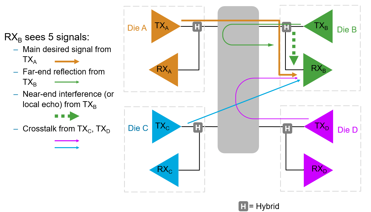
As chiplet interfaces scale toward higher data rates, SBD signaling—with its combination of doubled bandwidth density, low energy consumption, and reduced circuit complexity—represents a compelling solution for next-generation chip-to-chip interconnects.
IBIS-AMI for Simultaneous Bi-Directional Links
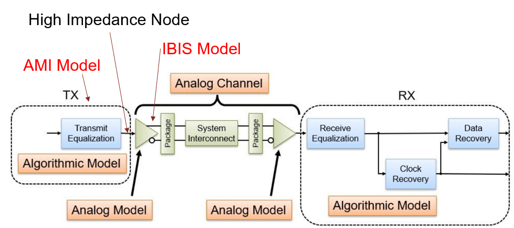
The IBIS-AMI framework is the industry standard for simulating high-speed serial links, enabling vendors to distribute accurate behavioral models without exposing proprietary circuit details. IC vendors compile their transmitter equalization, receiver equalization, and clock-data recovery algorithms into executable models that operate within an EDA tool's channel simulation environment. The compiled model reproduces proprietary transmitter and receiver behavior without disclosing its implementation details like the underlying circuit topology, process-technology parameters, and algorithmic details—providing system integrators with accurate behavioral models while protecting the transistor-level design and filter coefficients. The diagram below illustrates the unidirectional IBIS-AMI simulation components.
These same advantages apply with even greater importance to simultaneous bi-directional links. An SBD transceiver's core intellectual property resides in its echo cancellation architecture: the specific hybrid circuit topology, the adaptive algorithm that tracks echo cancellation tap weights, and the calibration sequence that converges the canceller at startup. Extending IBIS-AMI to SBD preserves the collaborative simulation workflow that the industry relies on for unidirectional links while protecting the proprietary IP that differentiates one vendor's echo-suppression strategy from another—a critical enabler as SBD transceivers transition from academic demonstrations toward production chiplet interfaces.
A key aspect of the IBIS-AMI framework is the high-impedance node that separates the analog circuit behavior (the IBIS portion) from the algorithmic behavior (the AMI portion). For unidirectional systems, this node is well defined. For SBD systems, however, the optimal placement of this boundary requires careful consideration. Some approaches introduce an additional hybrid S-Parameter, effectively placing much of the echo cancellation behavior outside the AMI model. In this implementation, the high-impedance node is positioned such that all echo suppression occurs within the compiled AMI model. This placement protects the echo-cancellation implementation and enables the AMI model to represent active and nonlinear behavior. The tradeoff is that certain analog circuit effects are approximated by mathematical operations inside the AMI model; however, as demonstrated in subsequent sections, these approximation errors can be minimized.
Representing the Nishi SBD Circuit with IBIS-AMI
Nishi et al. [1] use a replica driver to cancel local echo. A scaled copy (a "replica") of the transmit driver is fabricated on the same die. Because this replica is driven by the same outgoing data sequence, it produces an inverted version of the echo signal. The receiver combines this replica waveform with the received signal, thereby subtracting the self-interference component.
A key advantage of this approach is that the replica driver, fabricated adjacent to the main driver using the same process technology, inherently tracks variations in temperature, supply voltage, and manufacturing parameters. This eliminates the need for power-intensive digital filters, analog-to-digital converters, or complex calibration logic—the matching is maintained intrinsically through physical proximity and process correlation. This simplicity enables the complete transceiver to be constructed from basic CMOS inverter stages, achieving excellent energy efficiency. The design matches the energy efficiency of unidirectional links while delivering double the bandwidth per pin.
The limitation of this approach is that cancellation quality depends directly on the matching between the replica and main driver. It additionally cannot compensate for far-end echoes either. If the physical layout symmetry between the two drivers is imperfect, cancellation performance degrades. This constrains the technique to short, well-characterized channels—precisely the type found in silicon interposer die-to-die links—and makes it less suitable for longer or less predictable interconnect topologies.
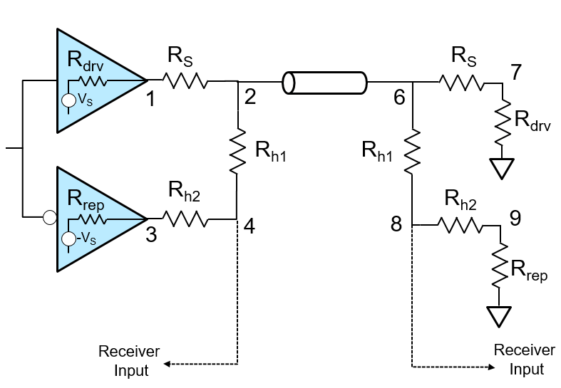
The SBD architecture utilized by Nishi is illustrated below. The main driver and an inverted replica driver of Die A are driven such that they cancel at the input to the Die A receiver, Vrx (or node 4). To model this circuit for the IBIS-AMI setup, also shown below, we configure the IBIS approximation circuit so that the loading of VtxA and VtxB is very similar to the Nishi circuit. This means that for the IBIS approximation circuit, the Vtx node becomes the high-impedance node that separates the IBIS from the AMI implementation.
To summarize, the IBIS approximation loads the high-impedance node with impedances that match the Nishi circuit as follows:
(transmitter output impedance)
(receiver input resistance including hybrid and replica)
The feedback resistor (1200 Ω) and the receiver amplifier visible in the Nishi circuit diagram do not appear in this derivation because they operate beyond the high-impedance node boundary. In the IBIS-AMI partitioning, and the amplifier are internal to the AMI model. Their high input impedance contributes negligible loading to the node.
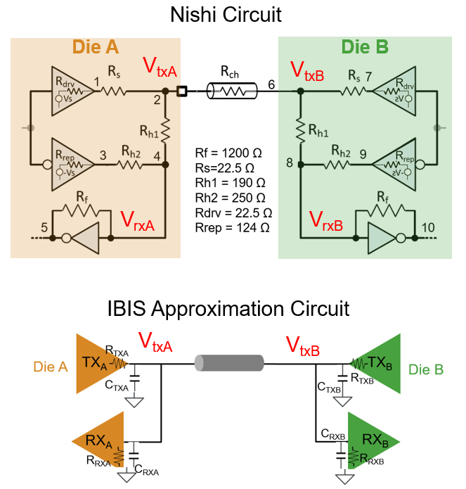
For the IBIS-AMI simulation, the receiver input node, Vrx, is internal to the AMI model. To determine this voltage, we take Vtx, the voltage at the output of the transmitter model, and scale Vtx by a factor dependent on the resistors Rh1, Rh2, Rs, Rdrv, and Rrep of the Nishi circuit. This scale factor is similar to, but not exactly, a voltage divider across Rh1.
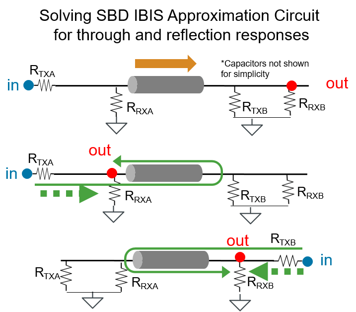
The process to extract the system impulse responses from the IBIS approximation circuit is illustrated in the following diagram for the through (S21) and reflection responses (S11 and S22). Note that the through response is represented by the orange arrow, the self-interference is shown by the large dotted green arrow, and the far-end reflection by the thin green arrow.
A fundamental limitation of the replica-based approach is its static nature—cancellation accuracy is determined by the initial layout match between the main and replica driver. The adjacent replica tracks correlated process, supply-voltage, and temperature variation, but spatial gradients, local supply differences, and aging mismatch leave residual error that degrades cancellation performance. Goyal et al.'s True Full-Duplex IO (TFD-IO) [2] addresses this limitation by implementing adaptive echo cancellation that operates continuously in the background. Rather than relying on a fixed replica, TFD-IO employs a feedback loop that correlates the transmitted data against the residual error at the receiver. Based on this correlation, the cancellation coefficients are updated continuously during normal data traffic—no interruption for recalibration is required. The system adapts autonomously as operating conditions change.
The result is echo cancellation that maintains accuracy over time, even as thermal conditions change, power supply noise increases, or components exhibit aging-related degradation. The tradeoff is that the adaptive approach requires additional digital filtering and correlation circuitry, which increases die area and introduces additional latency compared to the static replica method.
The model explored in the example embodies both the Nishi and Goyal approaches to demonstrate to the user how one or both approaches can be used for SBD links.
Simulink Model Architecture
The Simulink model, SimultaneousBiDirectional.slx, implements the SBD transceiver. Open it with the following command:
open_system('SimultaneousBiDirectional');
Each direction runs at 25 Gb/s (40 ps UI), for an aggregate bi-directional rate of 50 Gb/s.
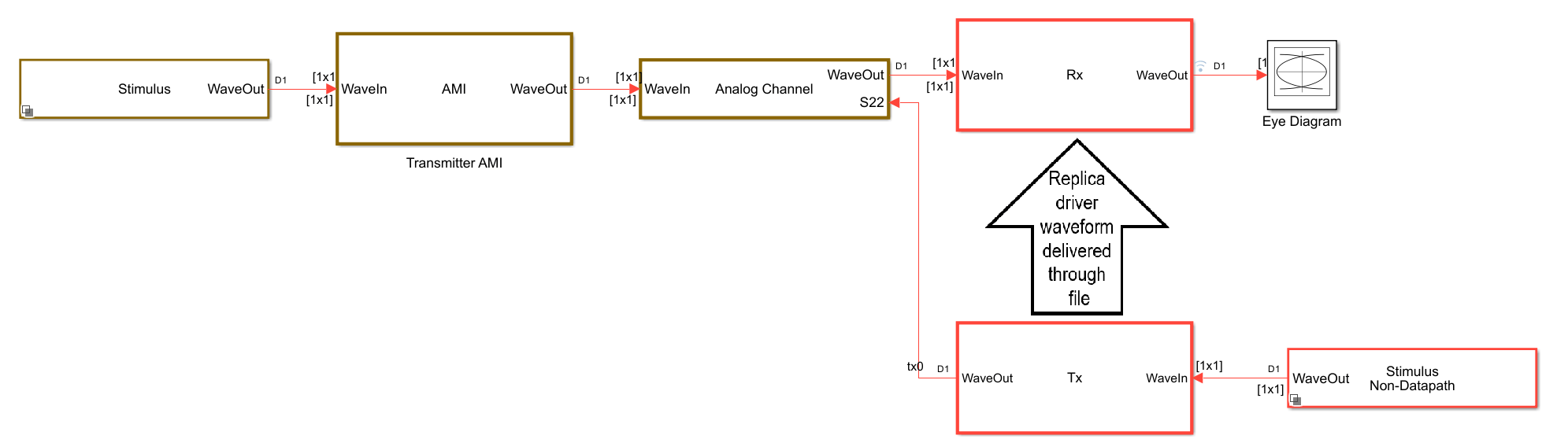
To simplify the SBD analysis, this example focuses on the right-side receiver. The model contains two subsystems on the right side (Tx and Rx) and an AMI block on the left side labeled Transmitter AMI. The SerDes Toolbox framework for IBIS-AMI model generation supports only a single Tx and Rx subsystem pair; the Transmitter AMI block represents an instance of the right-side Tx after AMI model generation. The analog channel combines the through and reflection responses before delivering the composite signal to the Rx. For echo cancellation, the right-side Tx must communicate its output waveform to the co-located Rx. This communication could be represented as an explicit signal wire in Simulink, but this approach is incompatible with AMI model generation due to limitations of the standard AMI interface. This implementation therefore uses a file-based communication mechanism: the Tx writes its waveform to a file, and the Rx reads that file during simulation.
Transmitter (Tx)
The transmitter subsystem is composed of several functional blocks. The FFE (Feed-Forward Equalizer) applies configurable tap weights for pre-emphasis signal conditioning. The DelayAndScale block provides two functions: it delays the transmitter output waveform for timing alignment, and it applies a scaling factor that facilitates debug and isolation testing. During troubleshooting, setting the scale factor to zero for either the left- or right-side transmitter removes its contribution from the composite signal, enabling independent analysis of each signal path. The ReplicaWriter block communicates the local Tx waveform to the co-located receiver through a waveform file, providing the echo reference signal required for cancellation.

Channel
To configure the channel, open the channel block mask and select the "Import S-Parameter Touchstone File" button to launch the S-Parameter Fitter app.
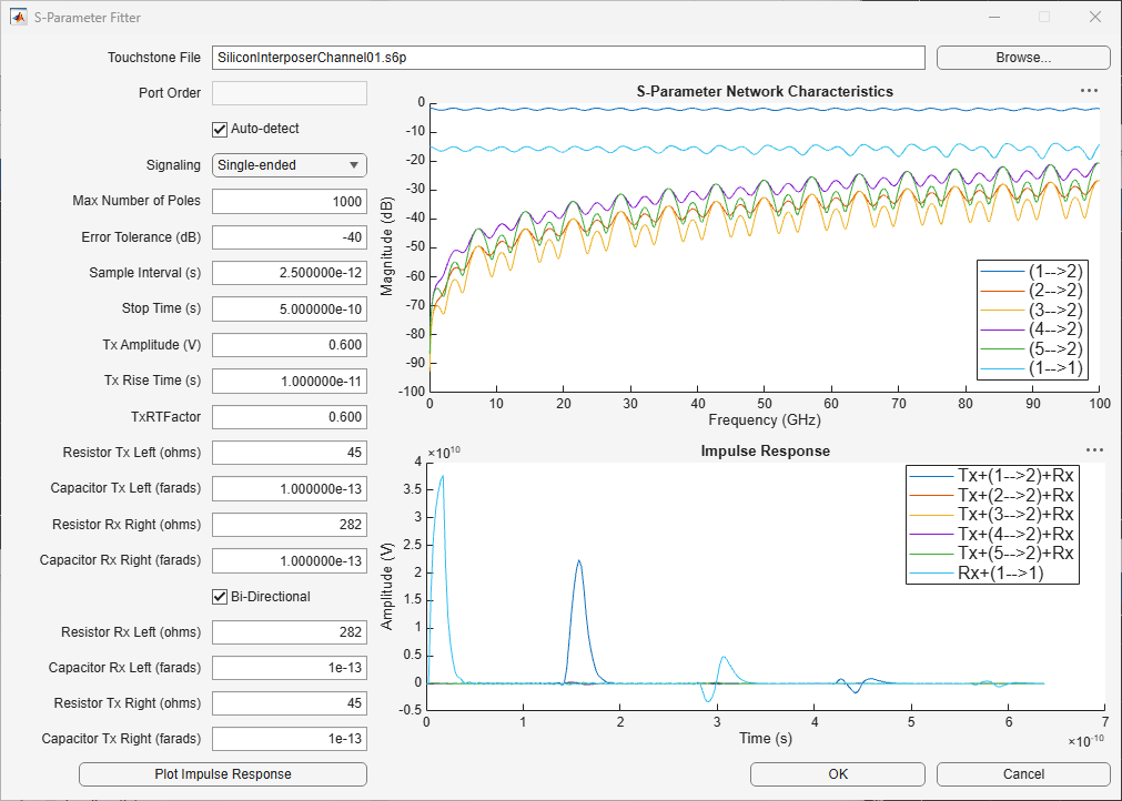
In the S-Parameter Fitter app, select SiliconInterposerChannel01.s6p. See Appendix B for the steps to generate this S-Parameter. For a single-ended SBD interface, this S-Parameter will contain the through, reflection and crosstalk responses.
Select Bi-Directional, and then enter 45 Ω for both left and right Tx source resistance and 282 Ω for both left and right Rx load resistance. See Appendix C for how these resistance values are determined. The app then computes the through impulse response, any crosstalk impulse responses from other transmitters, and the reflection impulse response. This reflection response includes both the self-interference behavior and the far-end reflection signal contribution.
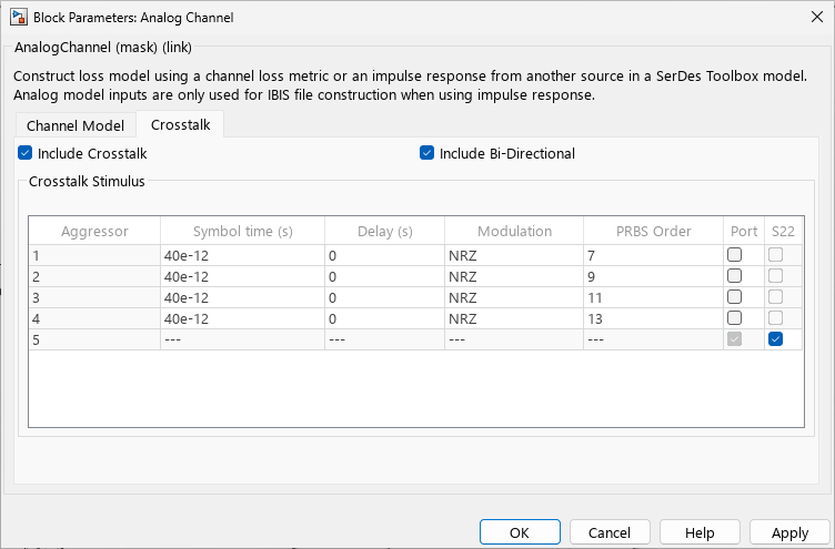
After pressing OK in the S-Parameter Fitter app, open the Analog Channel mask and select the crosstalk tab. This tab displays the stimulus configuration for the crosstalk aggressors and replica driver. Note that the last row has the "Port" and "S22" columns checked, indicating that it uses an external port and represents a reflection (S22) response.
Receiver (Rx)
The receiver has three subsystems: echo cancellation, CTLE, and a clock-forwarding block with DFE.

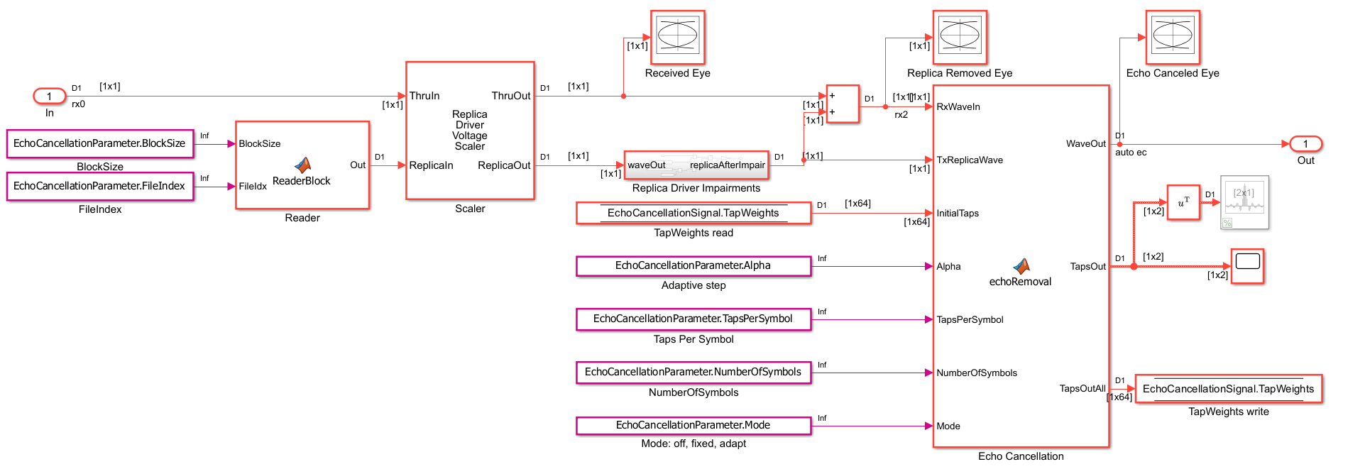
The echo cancellation subsystem contains multiple components, as shown in the image below.
Echo Cancellation
The Reader block takes in two AMI parameters, BlockSize and FileIndex. Using the value of FileIndex, it reads in the file, data_<FileIndex>.txt, which was written by the transmitter paired with this receiver. The replica driver waveform is obtained and passed along. This waveform transfer through a file mechanism is an example-specific approach inspired by the back-channel capabilities in IBIS-AMI where the receiver AMI model communicates with the transmitter AMI model. If multiple simulations are run concurrently, it will be important to set the FileIndex for each case to be distinct and independent to avoid data file collisions and corruption.
The ReplicaDriverVoltageScaler block estimates Vrx by multiplying the Vtx waveforms by a resistance-dependent scale factor.
The Replica Driver Impairments block exposes two AMI parameters, ReplicaGain and ReplicaDelay, which allow intentional gain or delay offsets to be injected into the replica driver waveform. These parameters enable sensitivity analysis of the system's tolerance to replica driver amplitude and timing mismatch. The model also uses ReplicaDelay to align the replica waveform with the S22 response.
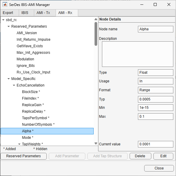
The Echo Cancellation block uses an FIR filter to delay and scale multiple copies of the replica driver waveform before combining it with the receiver input signal to cancel local echo and delayed reflected components. The FIR tap weight values are determined using the least mean squares (LMS) algorithm. The LMS algorithm operates by computing the correlation between the residual error at the output and the replica reference signal, then adjusting each tap weight in the direction that minimizes the mean-square error. The adaptation rate is governed by the Alpha parameter—smaller values of Alpha yield slower but more stable convergence, while larger values accelerate adaptation at the risk of instability. This adaptive filter refines the primary self-interference tap weight and cancels far-end echoes within its temporal reach.
The number of FIR filter taps is determined by the AMI parameters, TapsPerSymbol and NumberOfSymbols. The reach in time of the FIR filter is controlled by the NumberOfSymbols parameter, and the TapsPerSymbol parameter defines how the taps are spaced. The AMI parameter TapWeights defines a maximum of 64 taps and NumberOfSymbols*TapsPerSymbol must be less than or equal to 64. If more taps are desired, the TapWeights AMI parameter must be deleted in the IBIS-AMI Manager and a new longer tap structure added.
CTLE
Short interposer channels typically do not require significant equalization. In this configuration, the CTLE block is configured as a low-pass filter to attenuate high-frequency noise introduced by the echo canceller. It also serves as a placeholder for additional equalization that may be required for longer-reach channels.
Clock-forwarding block with DFE
In this configuration, the DFE equalization capabilities are disabled (DFE mode set to off). However, the clock forwarding functionality is active and models the forwarded clock employed in many die-to-die interfaces. The AMI parameter ForwardClockOffset controls the alignment between the clock and the data eye in the post-simulation Time Domain Analysis figure.
Modify AMI Parameters
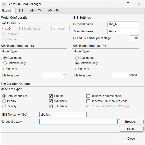
System parameters are configured through the top-level configuration block mask. Tx and Rx AMI parameters are configured using the SerDes IBIS-AMI Manager:
Run the Model
Click the run button to simulate the model and generate the following output figures.
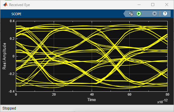
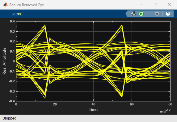
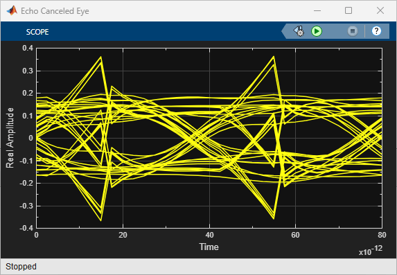
The received eye shows two NRZ signals superimposed, producing a multilevel pattern. Direct subtraction of the replica waveform in the "Replica Removed Eye" compensates for this, and the "Echo Canceled Eye" improves further as the first tap weight adjusts the magnitude of the subtracted replica. The model runs for 20,000 symbols (or 800 ns) but the tap weights fully converge after about 40,000 symbols (or 1,600 ns). To observe full convergence, increase the simulation length beyond the default.
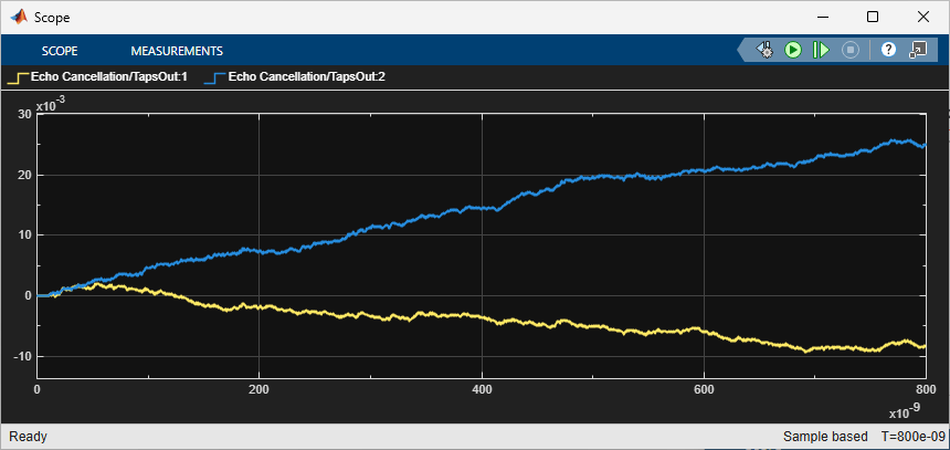
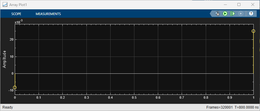
In this simulation, TapsPerSymbol is 1 and NumberOfSymbols is 2. The adaptive tap weights are shown above versus time and as an array plot versus the number of taps.
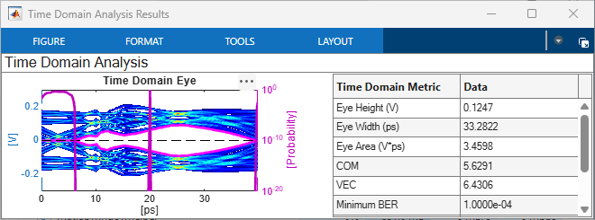
CTLE equalization improves the eye further (the DFE is not applied in this configuration). The clock forwarding parameter ForwardClockOffset is adjusted so that the clock signal in the Time Domain Analysis eye is well centered.
Export IBIS-AMI Model
Use the IBIS-AMI Manager to export paired transmitter and receiver IBIS-AMI models. After export, the compiled models can be used in any IBIS-AMI-compatible simulator that supports equivalent file-system access, block-size configuration, and model-execution order. The companion example, Simultaneous Bi-Directional Analysis in Parallel Link Designer (Signal Integrity Toolbox), demonstrates this workflow using Parallel Link Designer for system-level analysis.
Summary
This example demonstrates how to model simultaneous bi-directional die-to-die links within the SerDes Toolbox and IBIS-AMI framework.
SBD signaling doubles bandwidth density without adding pins, making it well suited for the pin-count-limited interfaces between chiplets in advanced packages. The IBIS-AMI modeling strategy places the hybrid circuit and echo cancellation inside the compiled AMI model, protecting sensitive IP while still enabling interoperable system-level simulation. A voltage scaling factor converts the IBIS high-impedance node voltage to the receiver sense amplifier voltage, bridging the gap between the standard IBIS analog model and the SBD-specific circuit topology. The Simulink architecture supports full-duplex SBD simulation by combining a transmitter (with FFE and replica writer), a channel with both through and reflection impulse responses, and a receiver with adaptive echo cancellation, CTLE, and clock-forwarded DFE.
The raw received eye resembles a multilevel signal because it contains the superposition of two NRZ data streams—the desired far-end signal and the local echo—demonstrating that the receiver input is a composite of multiple signal components before cancellation. Direct subtraction of the replica waveform removes the bulk of the echo, and the adaptive LMS algorithm further refines cancellation by compensating for gain and timing mismatches between the replica and the actual echo path. Even with a simple 2-tap canceller (1 tap per symbol over 2 UI), the adaptive algorithm begins to converge and improves the eye, demonstrating that short interposer channels require only modest cancellation complexity. CTLE provides additional eye opening after echo removal. The DFE is disabled in this configuration. The example therefore demonstrates echo cancellation, CTLE, and forwarded-clock operation, but does not evaluate whether DFE would provide additional margin.
Next Steps
Add crosstalk: Include S-Parameter channel models with aggressor ports to observe how crosstalk interacts with the echo and whether the canceller inadvertently suppresses or amplifies neighboring-lane interference.
Increase canceller complexity: Raise TapsPerSymbol and NumberOfSymbols to give the echo canceller more degrees of freedom. Setting TapsPerSymbol to 16 (matching samples per symbol) provides one cancellation tap per waveform sample and approximates a finely spaced cancellation response, revealing the practical limits of digital cancellation for a given channel.
Sweep the adaptation step size (Alpha): Try values ranging from 0.00001 to 0.01 to observe the tradeoff between convergence speed and steady-state residual error. Very small Alpha converges slowly but cleanly; large Alpha converges fast but may oscillate.
Introduce non-ideal replica matching: Adjust the ReplicaGain away from 1.0 and vary ReplicaDelay to simulate realistic mismatch between the replica driver and the actual echo path. Observe how much mismatch the adaptive algorithm can tolerate before the eye degrades.
Explore longer or lossier channels: Replace the silicon interposer channel with longer organic substrate or package models to test where the simple cancellation architecture breaks down and more aggressive equalization is needed.
Enable the DFE: Set the DFE tap weights to nonzero initial values or enable DFE adaptation to see if decision feedback provides additional margin after echo cancellation and CTLE, particularly for channels with more post-cursor ISI.
Multi-lane analysis in Parallel Link Designer: Export the IBIS-AMI models and build a widebus configuration with multiple SBD lanes to study system-level effects.
References
[1] Y. Nishi et al., "A 0.297-pJ/bit 50.4-Gb/s/wire inverter-based short-reach simultaneous bi-directional transceiver for die-to-die interface in 5-nm CMOS," IEEE J. Solid-State Circuits, vol. 58, no. 4, pp. 1062-1073, 2023.
[2] S. Goyal, G. Parulekar, and S. Gupta, "A true full-duplex IO (TFD-IO) with background SI cancellation for high-density interfaces," IEEE Trans. Very Large Scale Integr. (VLSI) Syst., vol. 30, no. 5, pp. 615-624, 2022.
Appendix A: SBD Simulink Troubleshooting
Establishing a functioning SBD link requires precise configuration, as multiple parameters must be correctly set for near-end interference and far-end reflections to be adequately suppressed. This section provides guidance for diagnosing common issues encountered during SBD link bring-up.
Symptom: Replica Removed Eye is not NRZ
The Replica Removed Eye looks similar or worse than the Received Eye (which typically looks like a multilevel eye).
File lock on waveform file — If the Simulink model is stopped mid-simulation, the simulation may terminate during a read or write operation on the waveform file, leaving it in a locked state. In subsequent simulations, the file lock prevents new waveforms from being written or read, effectively severing the communication path between the replica driver and the receiver.
Solution: Either manually delete the file data_<FileIndex>.txt or open the SerDes IBIS-AMI Manager and increment the FileIndex for both the transmitter and receiver AMI parameters.
Mismatched FileIndex/BlockSize — The FileIndex/BlockSize for the transmitter and receiver are not matched.
Solution: Verify that the FileIndex and BlockSize values are identical for both the transmitter and receiver.
Incorrect Scaler block parameters — The Scaler block in the receiver echo cancellation subsystem is not correctly scaling the through and replica waveforms.
Solution: Verify that the ReplicaDriverVoltageScaler block parameters (Rs, Rh1, Rh2, Rdrv, and Rrep) correspond to the RTX and RRX values returned by the scaler block and match the values used in the S-Parameter Fitter app.
Symptom: Cancellation glitch in center of eye
The cancellation artifact ("glitch") appears in the center of the eye.
Timing misalignment — Timing misalignment between the replica and echo paths.
Solution: Adjust the transmitter delay parameter. Note that proper transmitter delay adjustment requires consideration of both receivers in the system, not just one.
Symptom: Post-simulation eye misaligned with clock
The post-simulation Time Domain Analysis Results eye is misaligned with the clock.
Solution: Because the system uses clock forwarding, the data-to-clock alignment must be adjusted manually. Open the IBIS-AMI Manager, navigate to the AMI-Rx tab, select the DFEClkFwd block, and modify the ForwardClockOffset AMI parameter until the desired alignment is achieved.
General Recommendations
When using adaptive echo cancellation, verify that the "bits to ignore" setting is sufficiently large to allow the adaptation algorithm to converge adequately before waveform collection begins for eye diagram construction. The symbol error rate (SER) reported in the post-simulation Time Domain Analysis Results provides a useful metric for confirming that the received data pattern matches the transmitted data pattern.
Verify that the stimulus blocks for the left-side and right-side transmitters use different data patterns. If both use the 'Random Symbols' waveform creation method, assign different seed values to each transmitter.
Use the transmitter AMI parameter DelayAndScale.Scale to disable one transmitter at a time for isolation testing. Verify that an open eye can be obtained without the near-end interfering transmitter present. Alternatively, disable the left-side transmitter and examine the two signals at the adder block input to verify proper phase alignment. Both the transmitter and receiver subsystems provide delay adjustment capabilities.
Note that Appendices B through D are for reference and validation material and are not required for the core workflow.
Appendix B: Interposer Channel Creation
The following code creates a representative silicon interposer channel S-Parameter model.
% Baud frequency
fbaud = 12.5e9;

% Electrical line length in radians
lineLengthElectrical = 140e-12*2*pi;

% Line length
lineLength = lineLengthElectrical*fbaud;

% Channel DC resistance
Rch = 21.5;

% Coupling between lines for crosstalk. The number of such capacitors
% defines the number of aggressors
C1 = (1:2)*1e-15;

% Create circuit model: The through circuit consists of Rch/2 followed by
% half of the transmission line, followed by half the transmission line
% followed by Rch/2. Each aggressor is connected to the main through
% (ports 1 and 2) by their capacitor.
%
%
%             Rch/2      =======        =======      Rch/2
% port (1) o--/\/\/\----| TL/2  |------| TL/2  |----/\/\/\--o port (2)
%                    |   =======    |   =======   |
%                    |              |             |
%                  [Cap]          [Cap]         [Cap]
%                    |              |             |
%                    |              |             |
%             Rch/2  |   =======    |   =======   |  Rch/2
% port (3) o--/\/\/\----| TL/2  |------| TL/2  |----/\/\/\--o port (4)
%                        =======        =======

circuitModel = circuit;

% Victim through line.
add(circuitModel,[1 2],resistor(Rch/2));
add(circuitModel,[2 3],txlineElectricalLength(Z0=40,LineLength=lineLength/2,ReferenceFrequency=fbaud));
add(circuitModel,[3 4],txlineElectricalLength(Z0=40,LineLength=lineLength/2,ReferenceFrequency=fbaud));
add(circuitModel,[4 5],resistor(Rch/2));

% Keep track of the nodes that correspond to the S-Parameter ports.
NumberOfAggressors = length(C1);
ports = cell(1,NumberOfAggressors*2+2);
ports(1:2) = {[1 0],[5 0]};

% For each aggressor, create the through circuit and then connect it to the
% main through.
for ii = 1:NumberOfAggressors
    Node = ii*5+1;

    % Build through
    add(circuitModel,[Node+0 Node+1],resistor(Rch/2));
    add(circuitModel,[Node+1 Node+2],txlineElectricalLength(Z0=40,LineLength=lineLength/2,ReferenceFrequency=fbaud));
    add(circuitModel,[Node+2 Node+3],txlineElectricalLength(Z0=40,LineLength=lineLength/2,ReferenceFrequency=fbaud));
    add(circuitModel,[Node+3 Node+4],resistor(Rch/2));

    % Connect capacitor to main through
    add(circuitModel,[2,Node+1],capacitor(C1(ii)));
    add(circuitModel,[3,Node+2],capacitor(C1(ii)));
    add(circuitModel,[4,Node+3],capacitor(C1(ii)));

    % Keep track of which circuit nodes correspond to which ports.
    ports(ii*2+1) = {[Node 0]};
    ports(ii*2+2) = {[Node+4 0]};
end

% Define the ports in the circuit
setports(circuitModel,ports{:})

% Frequency uniformly spaced from 0 to 100 GHz
f = linspace(0,100e9,1001*2);

% Generate S-Parameter
Sparameter = sparameters(circuitModel, f,50);

% Write S-Parameter to file
fn = sprintf('SiliconInterposerChannel01.s%ip',Sparameter.NumPorts);
if ~exist(fn,'file')==2
    rfwrite(Sparameter,fn);
end

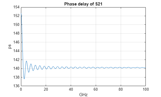
%% Visualize through loss, return loss, NEXT and FEXT

s21 = squeeze(Sparameter.Parameters(2,1,:));
s11 = squeeze(Sparameter.Parameters(1,1,:));

% Calculate phase delay
pds21 = -unwrap(angle(s21))./(2*pi*f');

% Extract far and near end crosstalk
fext = zeros(length(f),NumberOfAggressors);
next = zeros(length(f),NumberOfAggressors);
fextlbl = cell(1,NumberOfAggressors);
nextlbl = cell(1,NumberOfAggressors);
for ii = 1:NumberOfAggressors
    fext(:,ii) = squeeze(Sparameter.Parameters((ii+1)*2,2,:));
    fextlbl{ii} = sprintf('FEXT: S_{%i,%i}',(ii+1)*2,2);
    next(:,ii) = squeeze(Sparameter.Parameters((ii+1)*2-1,2,:));
    nextlbl{ii} = sprintf('NEXT: S_{%i,%i}',(ii+1)*2-1,2);
end

% Visualize responses
fg = f*1e-9;

plot(fg,pds21*1e12),
grid on,ylabel('ps'),xlabel('GHz')
title('Phase delay of S21')
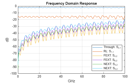
plot(fg,db(s21),fg,db(s11),fg,db(fext),fg,db(next))
grid on
xlabel('GHz'),ylabel('dB')
hLeg = legend(['Through: S_{2,1}','RL: S_{1,1}',fextlbl,nextlbl],'location','southeast');
hLeg.ItemHitFcn = @ctlefit.ToggleLineVisibility;
title('Frequency Domain Response')
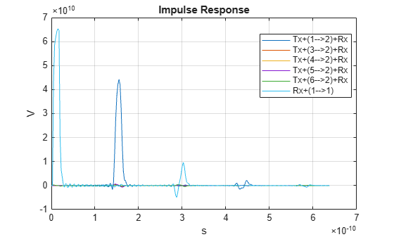
% Visualize impulse responses
SymbolTime = 40e-12;
SampleInterval = SymbolTime/16;
C2 = 50e-15;

obj1 = SParameterChannel(...
    'FileName',fn,...
    'Signaling','single-ended',...
    'StopTime', 0.2e-9,...
    'BiDirectionalModel','ReplicaSummer',...
    'SampleInterval',SampleInterval,...
    'ResistorTxLeft', 45,...
    'CapacitorTxLeft', C2,...
    'ResistorRxRight', 282,...
    'CapacitorRxRight', C2,...
    'ResistorRxLeft',282,...
    'CapacitorRxLeft',C2,...
    'ResistorTxRight', 45,...
    'CapacitorTxRight', C2,...
    'TxRiseTime',SymbolTime/4);

plotImpulse(obj1)
Appendix C: IBIS Approximation Circuit Validation
As discussed in the main body section of the example, the Nishi [1] SBD circuit is simplified to better conform with the IBIS-AMI requirement of a single high-impedance node to separate the IBIS portion of the model from the AMI portion of the model. In this section we illustrate the accuracy of this choice through circuit simulations. We include here again the figure that illustrates the full Nishi SBD circuit and the IBIS approximation circuit.
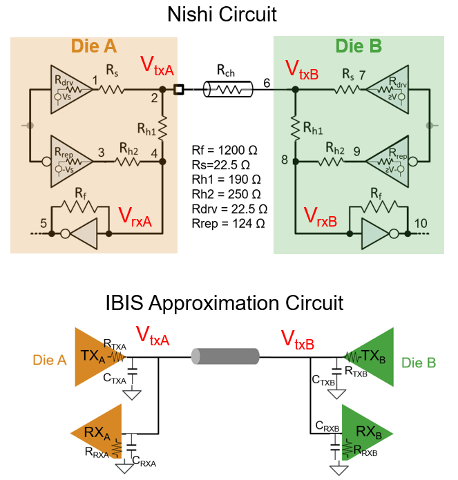
The following diagram of the Nishi circuit is implemented below in a HSPICE netlist.
* Nishi Circuit Simultaneous BiDir System
*
* Positive and complementary stimulus:
*
Vv_stimulus   v_stimulus   0 DC=0.  pwl( 0 0. +1.00000E-10 0. +1.00500E-10 .5 +1.01000E-10 1.  +1.01000E-08 1. )
Vv_stimulus_N v_stimulus_N 0 DC=1.  pwl( 0 1. +1.00000E-10 1. +1.00500E-10 .5 +1.01000E-10 0.  +1.01000E-08 0. )
*
.temp = 25
.tran 2pS 14.1nS
VTimeStep TimeStep 0 DC 1.
TTimeStep TimeStep 0 0 0 Zo=50. TD=2p
.options post probe dvdt=3
.option delmax=2ps
*
*** Parameter definitions for the circuit ***
*   Rs       = 22.5 ohm  Source resistance
*   Rh1      = 190  ohm  Hybrid resistor 1
*   Rh2      = 250  ohm  Hybrid resistor 2
*   Rdrv     = 22.5 ohm  Driver resistance
*   Rrep     = 124  ohm  Replica driver resistance
*
.param Rs   = 22.5
.param Rh1  = 190
.param Rh2  = 250
.param Rdrv = 22.5
.param Rrep = 124
*
* Near-end driver and replica resistors:
RdrvA v_stimulus   1 Rdrv
RrepA v_stimulus_N 3 Rrep
*
* Near-end hybrid network:
RsA  1 2 Rs
Rh1A 2 4 Rh1
Rh2A 3 4 Rh2
*
* Channel-model
.model s_model S TSTONEFILE='SerDesExample01sub12.s2p'
S1 2 0 6 0 mname=s_model
*
* Far-end hybrid network:
RsB  6 7 Rs
Rh1B 6 8 Rh1
Rh2B 8 9 Rh2
*
* Far-end quiet termination: far-end driver held quiet (0V).
RdrvB 0 7 Rdrv
RrepB 0 9 Rrep
*
* Probe statements: specify which signals to save
.probe tran v(v_stimulus)
.probe tran v(v_stimulus_N)
.probe tran v(4)
.probe tran v(2)
.probe tran v(6)
.probe tran v(8)

.END
To validate the approximation, compare the voltages at VtxA and VtxB (transmitter nodes 2 and 6 from HSPICE), SParameterChannel, and Parallel Link Designer. Below the HSPICE results are extracted from the simulation results.
% Replica Driver HSPICE results
waveData = tr0Reader('sbd_Nishi.tr0');

tSim = double(waveData{:,1});
v_stimulus = double(waveData{:,2});
v_stimulus_n = double(waveData{:,3});
vrx4 = double(waveData{:,4});
vpad2 = double(waveData{:,5});
vpad6 = double(waveData{:,6});
vrx8 = double(waveData{:,7});
The SParameterChannel class is used by the SerDes Toolbox to extract the impulse response from an S-Parameter with transmitter and receiver capacitances and resistances.
% Define nominal resistor values.
Rdrv = 22.5;
Rs = 22.5;
Rh1 = 190;
Rh2 = 250;
Rrep = 124;

% Define S-Parameter file
ChannelSParameterFileName = 'SerDesExample01sub12.s2p';

% Define system parameters
SampleInterval = 3.5e-12;
StopTime = 8e-9; % stop time

% Calculate IBIS approximation transmitter and receiver effective
% resistances.
Rtx = Rdrv + Rs;
Rrx = (Rh1+Rh2+Rrep)/2;

% Set amplitude to half for single-ended signaling.
TxAmplitude = 1/2;

% SParameterChannel
scobj = SParameterChannel(...
    'FileName',ChannelSParameterFileName,...
    'Signaling','single-ended',...
    'StopTime', StopTime,...
    'TxRiseTime', 20e-12,...
    'AggressorDefinition','same-load',...
    'SampleInterval',SampleInterval,...
    'BiDirectionalModel','ReplicaSummer',...
    'ResistorTxLeft', Rtx,...
    'CapacitorTxLeft', 1e-13*0,...
    'ResistorRxLeft', Rrx,...
    'CapacitorRxLeft', 1e-13*0,...
    'TxAmplitude', TxAmplitude,...
    'ResistorRxRight', Rrx,...
    'CapacitorRxRight', 2e-13*0,...
    'ResistorTxRight', Rtx,...
    'CapacitorTxRight', 1e-13*0);

% Extract the impulse and time vectors from the SParameter Channel:
ir = scobj.ImpulseResponse;
tSPC = SampleInterval*(0:length(ir)-1);
sr = impulse2step(ir,SampleInterval);
stepThruSPC = sr(:,1);
stepReflectSPC = sr(:,2);
The Parallel Link Designer project, utilized by the Simultaneous Bi-Directional Analysis in Parallel Link Designer (Signal Integrity Toolbox) example, contains a sheet that we reference here to illustrate the accuracy of the IBIS approximation.
% Get PLD waveforms from Parallel Link Designer project
PLDProjectPath = fullfile(pwd,'SBDExamplePLD');
try
    sip = SignalIntegrityProject(PLDProjectPath,readOnly=true);
catch ME
    % if path is not a Signal Integrity Project, then download kit
    if (strcmp(ME.identifier,'si:apps:NotAProject'))||(strcmp(ME.identifier,'MATLAB:validators:mustBeFolder'))
        fprintf('Parallel Link Project not detected, downloading SBDExamplePLD.zip from KIT repository\n')

        openSignalIntegrityKit('SBDExamplePLD',PLDProjectPath);

        sip = SignalIntegrityProject(PLDProjectPath);
    else
        % Failed for other reasons
        rethrow(ME)
    end
end

% The sheet 'sbd02' uses the S-Parameter SerDesExample01sub12.s2p and
% contains the simulated step responses.
sh = sheet(sip,'sbd02');

% Get list of simulation files.
simAll = sh.simData(type="Spice");

% Get the through and reflection waveforms
wavePLDFileIndex = find(~cellfun(@isempty,regexp([simAll.path],'tx_ttte.csd$')));
wavePLDTable = si.utilities.csdReader(simAll(wavePLDFileIndex(1)).path);
tPLD = wavePLDTable.('time');
stepThruPLD = wavePLDTable.('V(rx_g1_pad)');
stepReflectPLD = wavePLDTable.('V(tx_g1_pad)');

% Release Signal Integrity project object
sip.exit;
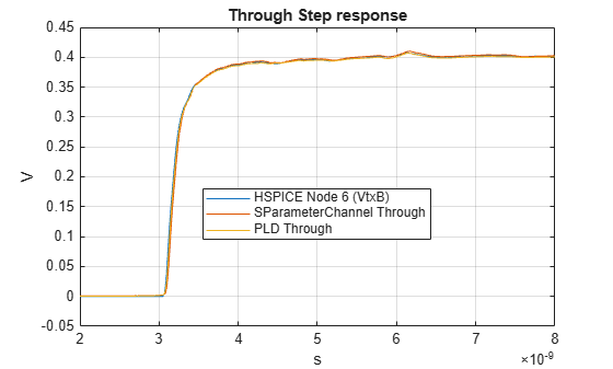
The left-side to the right-side through response of the Nishi HSPICE circuit, the SParameterChannel and the PLD simulator are compared below. These show very good correspondence in voltage swing and location of impedance discontinuities of the S-Parameter. Click the legend of the figure to toggle the line visibility for easier comparison.
% Remove known stimulus onset delays from each simulator so that the
% response edges align at t=0. The HSPICE stimulus begins at 100 ps
% (defined in the .pwl source) and PLD applies a 200 ps setup interval
% before the stimulus transition.
spiceDelay = 100e-12;
pldDelay = 200e-12;

% Compare waveforms in a plot
plot(tSim-spiceDelay,vpad6-vpad6(1),...
    tSPC,stepThruSPC,...
    tPLD-pldDelay,stepThruPLD);
title('Through Step response')
xlabel('s')
ylabel('V')
hLeg1 = legend({'HSPICE Node 6 (VtxB)','SParameterChannel Through','PLD Through'},...
                'interpreter','none','location','best');
hLeg1.ItemHitFcn = @ctlefit.ToggleLineVisibility;
grid on
xlim([2e-9 8e-9])
The following plot compares the three reflection responses. They have similar shapes and reflection timing, although their DC levels differ.
plot(tSim-spiceDelay,vpad2,...
     tSPC,stepReflectSPC,...
     tPLD-pldDelay,stepReflectPLD)
Warning: Graphics acceleration hardware is unavailable. Graphics quality and performance might be diminished. See <a href="https://www.mathworks.com/support/requirements/matlab-system-requirements.html">MATLAB System Requirements</a>.
title('Reflection Step response')
xlabel('s')
ylabel('V')
hLeg2 = legend({'HSPICE Node 2 (VtxA)','SParameterChannel Reflection','PLD Reflection'},...
    'interpreter','none','location','best');
hLeg2.ItemHitFcn = @ctlefit.ToggleLineVisibility;
grid on
xlim([-100e-12 6e-9])
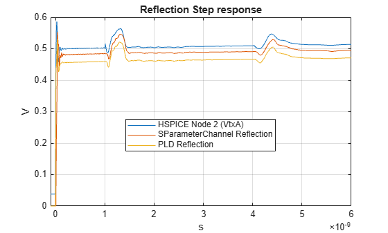
The through responses show close agreement across all three representations. The reflection responses exhibit similar transient shape and timing but retain a small DC-level offset between HSPICE and the IBIS approximation. This offset arises because the IBIS approximation circuit does not model the quiescent bias point of the Nishi hybrid network. The echo cancellation receiver is insensitive to this DC offset because the adaptive FIR filter operates on AC-coupled signal variations and the LMS algorithm converges on the time-varying echo component regardless of the absolute DC level.
Appendix D: Vtx to Vrx Scale Factor Determination Method
Appendix C shows that the IBIS approximation circuit can capture the transmitter pad voltages accurately at VtxA and VtxB. But to determine the receiver input voltage, VrxA and VrxB, we need to apply a scale factor inside the receiver AMI model. How this factor was determined is illustrated here. When consulting the Nishi circuit diagram, it appears that determining node 8 behavior from observations of node 6 voltage would be a simple voltage divider, but the relationship is a bit more involved.
First, verify the scale factor returned by ReplicaDriverVoltageScaler. Then, derive the fitted expression used by the object.
% Determine scaling factor dependent on the hybrid network resistance
% values.
ScaleObj = ReplicaDriverVoltageScaler(Rs=22.5,Rh1=190,Rh2=250,Rdrv=22.5,Rrep=124);

% Report scale factor
scaleFactor = ScaleObj.ThruGain;
fprintf('Scale factor = %g\n',scaleFactor)
Scale factor = 0.662852
% Report transmitter effective resistance
fprintf('Transmitter effective resistance = %g Ohms\n',ScaleObj.RTX)
Transmitter effective resistance = 45 Ohms
fprintf('Receiver effective resistance = %g Ohms\n',ScaleObj.RRX)Receiver effective resistance = 282 Ohms
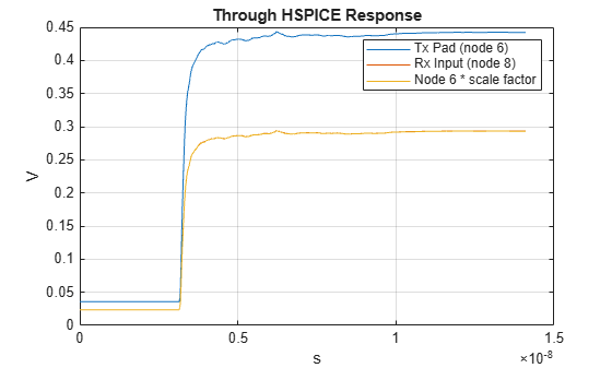
In the following plot we show that for the through response, the simulated receiver input waveform can be well approximated by a scaled version of the pad node voltage. Clicking on the legend labels will toggle the visibility of the waveforms, allowing for a simple way to compare results.
plot(tSim,vpad6,tSim,vrx8,tSim,vpad6*scaleFactor)
grid on
ylabel('V')
xlabel('s')
hLeg3 = legend('Tx Pad (node 6)','Rx Input (node 8)','Node 6 * scale factor');
hLeg3.ItemHitFcn = @ctlefit.ToggleLineVisibility;
title('Through HSPICE Response')
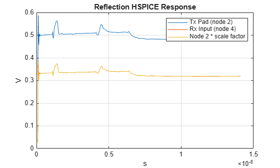
The same scale factor when applied to the reflection response illustrates how the receiver input voltage is well approximated by a scaled version of the pad voltage.
plot(tSim,vpad2,tSim,vrx4,tSim,vpad2*scaleFactor)
hLeg4 = legend('Tx Pad (node 2)','Rx Input (node 4)','Node 2 * scale factor');
hLeg4.ItemHitFcn = @ctlefit.ToggleLineVisibility;
grid on
ylabel('V')
xlabel('s')
title('Reflection HSPICE Response')
To determine this scaling factor across the space of possibilities of Rs, Rh1, Rh2, Rrep, Rdrv, we performed a design of experiments (DOE). Across 300 variations of the input parameters, the Nishi circuit was simulated and the scale factor needed to multiply the pad voltage (VtxA or VtxB) to the receiver input voltage (VrxA or VrxB) was extracted. The following code segments require the Statistics and Machine Learning Toolbox and are included (but not run here) for your reference.
% Define the nominal value of each factor
Rs   = 22.5;
Rh1  = 190;
Rh2  = 250;
Rdrv = 22.5;
Rrep = 124;

% Define the number of runs
nruns = 300;

% Define the factor bounds
bounds = [Rs*0.8, Rh1*0.8, Rh2*0.8, Rdrv*0.8, Rrep*0.8; ... % Lower bounds of factors
          Rs*1.2, Rh1*1.2, Rh2*1.2, Rdrv*1.2, Rrep*1.2];    % Upper bounds of factors

% Create design of experiments
dopt = optimalDOE(bounds,nruns,...
    AvoidDuplicates=true,...
    ModelSpecification='quadratic',...
    NumTries = 5,...
    FactorNames=["Rs", "Rh1", "Rh2","Rdrv","Rrep"]);
For each row in the table dopt.Design, insert the values of Rs, Rh1, Rh2, Rdrv and Rrep into the HSPICE netlist. Simulate, calculate and record the scale factor needed to transform the transmitter pad VtxB (node 6) to the receiver input VrxB (node 8). The results of such a process are contained in the example file "DesignOfExperimentsData.mat".
% Load design and scale factor data
DOEData = load('DesignOfExperimentsData.mat');
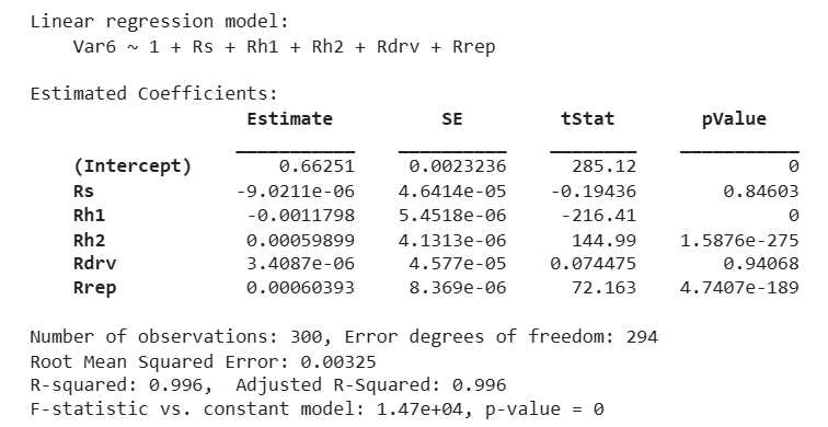
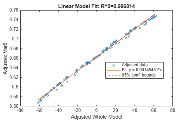
While the above design of experiments includes enough data for a quadratic fit, a linear fit was sufficient to capture the majority of the circuit scaling behavior. A sensible guideline to follow whenever fitting a model to data is to utilize the simplest model that sufficiently captures the desired behavior. A lower-order model reduces unnecessary complexity and can generalize better between the simulated design points. As observed below, the large p-values of Rs and Rdrv indicate that these terms contribute minimally to prediction accuracy. However, all five physical resistor terms are deliberately retained in the final scale function because they maintain a direct correspondence to the circuit topology. This ensures the model remains physically interpretable and correctly responds if future operating conditions shift Rs or Rdrv outside the range explored here.
DOEModelFit = fitlm(addvars(DOEData.dopt.Design,DOEData.ScaleObserved),'linear');
disp(DOEModelFit)
plot(DOEModelFit),
title(sprintf('Linear Model Fit: R^2=%g',DOEModelFit.Rsquared.Ordinary))
plotResiduals(DOEModelFit,'caseorder')
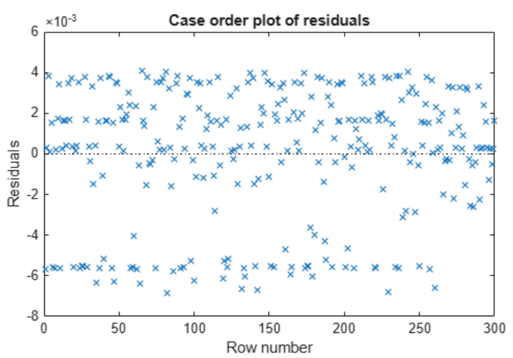
The residual plot exhibits banding patterns characteristic of a discrete factorial design. Over the ±20% variation range around nominal resistor values, the linear model achieves a maximum absolute error of less than 7e-3 in the scale factor. This error is small relative to the scale factor magnitude (~0.66) and contributes negligible distortion to the echo-cancelled eye.
Use the fitted coefficients to define a function that implements the linear fit model.
ScaleFunction = @( Rs, Rh1, Rh2, Rdrv, Rrep) [1 Rs Rh1, Rh2, Rdrv, Rrep]*[0.662510;-9.021115e-06;-0.001179;0.0005989;3.4087367e-06;0.0006039];
When evaluating this scale factor function at the nominal factor values, we see that we get the same scale value as we assumed at the beginning of this appendix.
ScaleFunction( Rs, Rh1, Rh2, Rdrv, Rrep)
ans =
    0.6630
This appendix has shown the necessity of using a scale factor to translate VtxB to VrxB and VtxA to VrxA as well as a method for determining the scale factor.

