Simultaneous Bi-Directional Analysis in Parallel Link Designer
R2026bThis example shows how to take the compiled IBIS-AMI models exported in the Simultaneous Bi-Directional Analysis in Simulink (SerDes Toolbox) example and integrate them into Parallel Link Designer for system-level analysis of a simultaneous bi-directional die-to-die link. While the Simulink-based workflow gives you full visibility into the transceiver's internal behavior, internal nodes and intermediate eye diagrams, Parallel Link Designer provides the system integrator's perspective: how does this link perform when embedded in a realistic multi-lane topology? You will import the SBD transmitter and receiver AMI models, configure the channel with the silicon interposer S-parameter, set up the bi-directional simulation environment so that both directions share a common channel, and run time-domain analyses to evaluate link margin. This workflow mirrors how silicon IP vendors and system integrators collaborate in practice—the vendor delivers compiled AMI models that protect echo cancellation IP, and the integrator evaluates system-level performance without needing access to the underlying circuit design.
Simultaneous Bi-Directional Links
As transistor scaling approaches physical limits, the semiconductor industry has adopted chiplet-based architectures—partitioning monolithic dies into smaller specialized dies interconnected within a single package under standards like UCIe. The inter-chiplet interconnects then become the bandwidth bottleneck due to limited bump pitch. Simultaneous bi-directional (SBD) signaling addresses this by transmitting data in both directions on the same conductor concurrently, doubling throughput per pin without additional connections. Unlike PAM-4, which also doubles data rate but often requires power-hungry FEC to recover margin due to reduced voltage levels, SBD retains simple NRZ modulation in each direction, retaining binary signaling and full voltage swing per transmitted symbol while enabling low-power driver circuits.
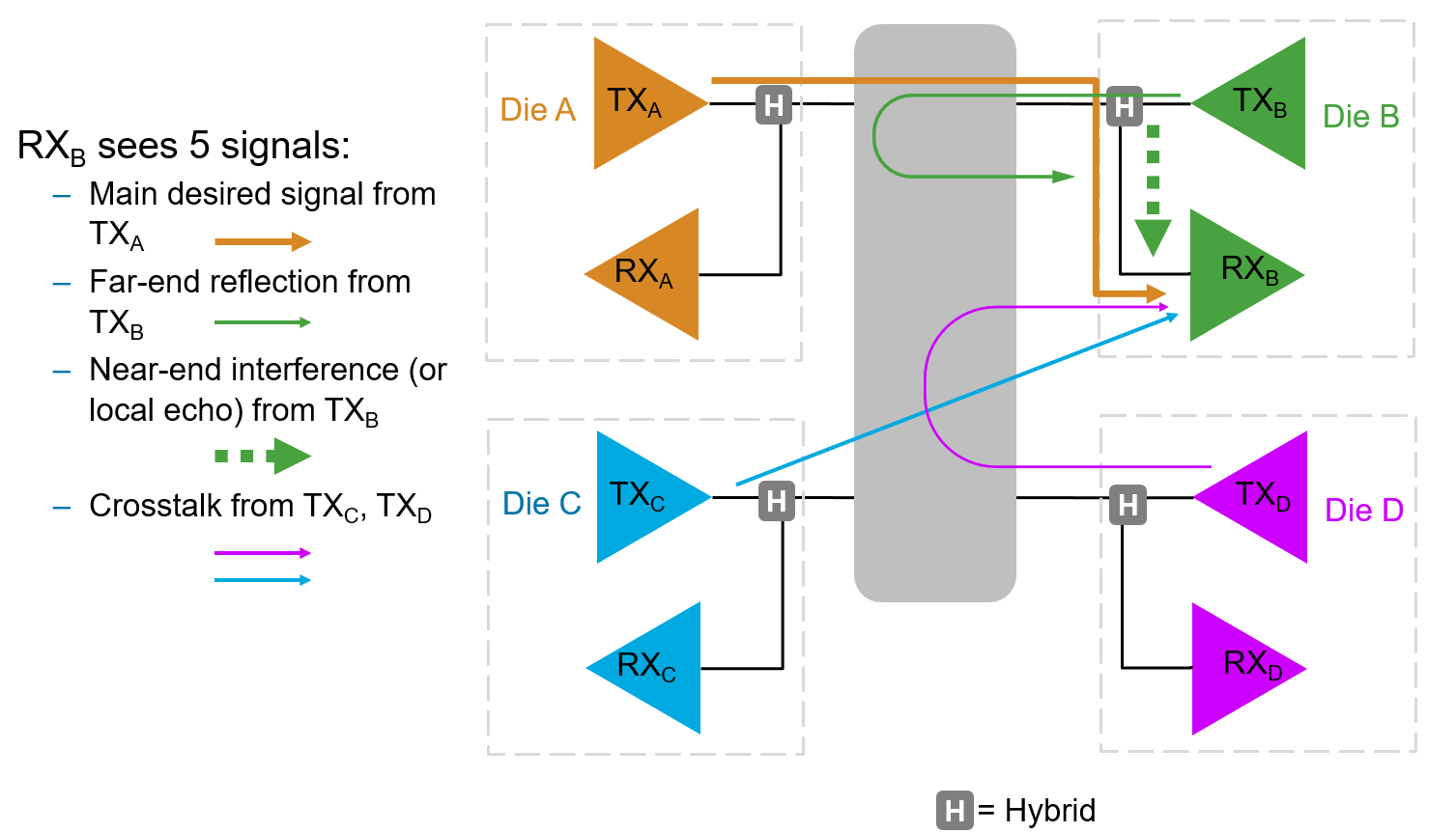
The diagram below illustrates the signal environment at receiver RXB. The desired signal arrives from the far-end transmitter TXA (the signal RXB must recover), but superimposed on it are two interference components from the co-located TXB: the self-interference (local echo reflecting back from the near-end driver) and the far-end echo (the TXB signal reflecting off impedance discontinuities at the far end of the channel). Additionally, crosstalk from adjacent transmitters in the system contributes further corruption. The receiver's task is to recover the desired TXA data signal in the presence of these unwanted components. The echo cancellation architecture cancels the self-interference and far-end echo using the local transmitter reference, while crosstalk from adjacent lanes is managed through signal margin.
Get Example SBD Parallel Link Designer Project
The following command will download and open the example project.
PLDProjectPath = fullfile(pwd,'SBDExamplePLD');
openSignalIntegrityKit('SBDExamplePLD',PLDProjectPath);
Run the Simulation and Interpret Results
Simulate the widebus sheet 'sbd01'. Ensure that 'Perform Channel Analysis' is checked in the SI/Timing Simulation Steps.
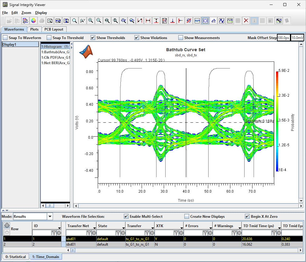
The resulting simulation has two simulation results displayed in the Signal Integrity Viewer. Note the column labeled "XTK" in the results table. This is an indication of the inclusion of crosstalk in the simulation, but due to the unique configuration we have set up, this is an indication that simultaneous bi-directional analysis has been done. The two results will be helpful when trying to understand the system performance with and without interference.
Select the first result row, right-click and select "Show BER" to display the BER eye.
To visualize the time domain waveforms:
Create a new display
Right-click in the display region (near the string "Display1") and select "Add new Display"
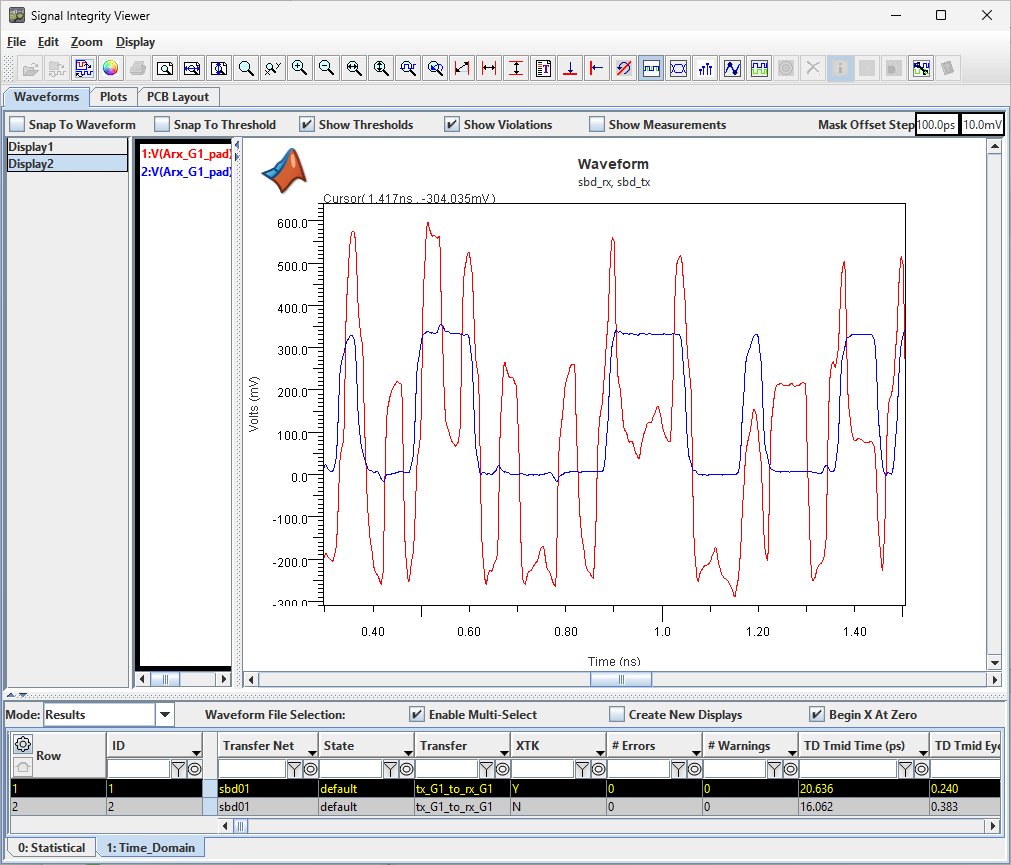
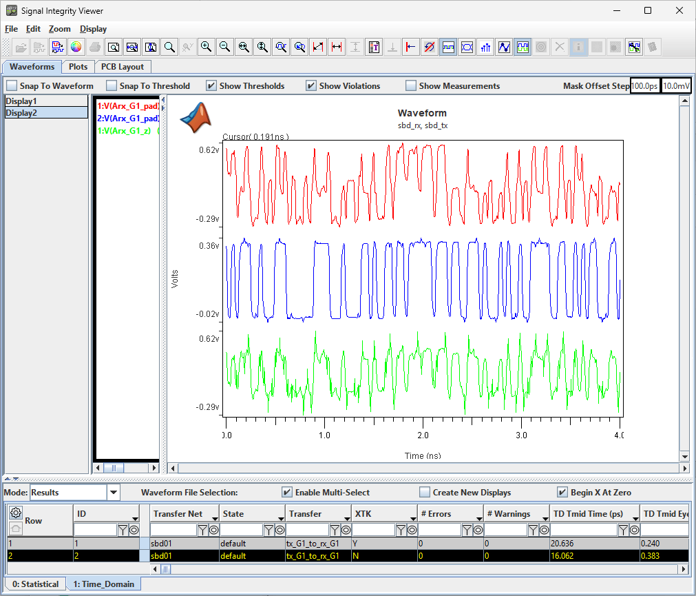
Select both rows 1 and 2 > right-click > Show Waveform > BRX to visualize the waveforms for each simulation just before the receiver as shown below.
This figure shows the SBD receiver input in red and the without-interference input in blue. The blue waveform is what we are trying to estimate from the red waveform.
Add the waveform after the receiver echo cancellation to the figure.
Right-click on row 1 > Show Waveform > ARX
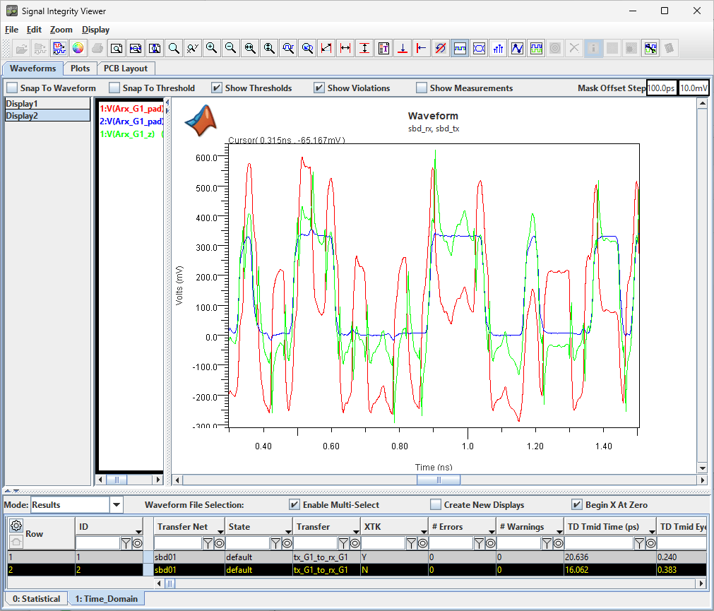
Choose the split view to see the three waveforms separated vertically.
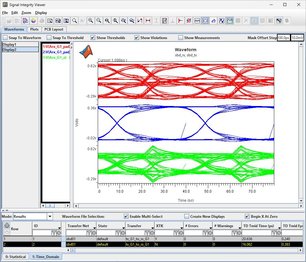
Press the "Eye Mode" button to compare the eye for the three waveforms.
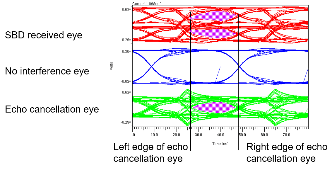
Consider the edges of the echo cancellation eye and you can start to identify which parts of the SBD received eye are extracted through the echo cancellation process. These areas are highlighted below with a purple hashed pattern.
Next Steps
Explore with different Replica delays in rx_G1. Try a sweep of values from 0 to 15e-12 in steps of 2.5e-12.
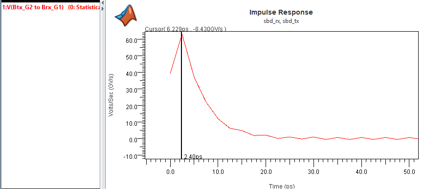
The Replica delay parameter of the receiver is used here to align the transmitter tx_G2 waveform with the near-end echo present in the received waveform so that the subtraction works well. If you examine the unequalized impulse response of the interference, labeled V(Btx_G2 to Brx_G1), you can see that the peak occurs at about 2.5 ps, which gives the largest eye opening for the above sweep of Replica delays. Future versions of the SBD AMI model will account for this parameter automatically by analyzing the interference impulse response in AMI_Init and then utilizing this value in AMI_GetWave.
Try a different channel.
Be sure to observe the impulse response of the interference so that you can correctly align the replica driver with the echo interference.
Try with more echo cancellation taps.
Increase rx_G1:EchoCancellation.TapsPerSymbol and rx_G1:EchoCancellation.NumberOfSymbols. Note that for this particular AMI model, TapsPerSymbol*NumberOfSymbols needs to be less than or equal to 64. Experiment with different values of Alpha to balance convergence time with settling noise.
Plot the tap values versus time by plotting the output AMI parameters for rx_G1.
Experiment with adding transmitter jitter.
Explore changing the transmitter delay capabilities and see how the echo cancellation eye grows or shrinks. Is there an optimal delay?
Troubleshooting Tips for SBD PLD Simulations
To visualize the signal without interference, view the simulation results for "N" crosstalk.
Each transmitter has a "DelayAndScale.Scale" variable which can be used to turn off any particular transmitter if you are trying to isolate a particular signal. Sweeping a scale from 0 to 1 can be insightful.
Double-check that FileIndex and BlockSize are set properly for the pair of transmitter and receiver to communicate the replica driver waveform. Also ensure that other transmitters have different FileIndex values.
Double-check that the receiver ReplicaDelay value corresponds to the channel reflection impulse response delay.
Summary
This example demonstrated how to integrate compiled SBD IBIS-AMI models into Parallel Link Designer for system-level analysis of a simultaneous bi-directional die-to-die link. The widebus sheet configuration enables simulation of both the desired through signal and the self-interference on a shared channel. The current configuration analyzes one direction of the bi-directional link; the opposite direction can be evaluated by designating the complementary transmitter-receiver pair as the victim.
Appendix: Creating the SBD PLD Project
This section details the steps taken to create the widebus sheet in the example PLD project provided. The steps are included here so you can better recreate these results with your own transceiver AMI models and channels. Widebus sheets enable the inclusion of multiple transmitters into one simulation, and while traditionally used for crosstalk analysis, here we leverage them to enable SBD analysis. For each transfer pair in the widebus sheet, an "associated sheet" is required to define the transmitter/receiver models. These sheets do not need to be simulated and are used for definition purposes only. The full recreation steps are as follows:
Create new Parallel Link Designer project
Import IBIS-AMI Models from the SerDes Toolbox example, Simultaneous Bi-Directional Analysis in Simulink (SerDes Toolbox).
Libraries > Import IBIS ... > Browse to
sbd.ibsfile
Import channel S-Parameter
Libraries > Import S-Parameter ... > Browse to SiliconInterposerChannel01.s6p in example directory.
Create associated sheets in preparation for Widebus analysis.
Create sheet
File > Schematic Sheet > New Sheet ...
Name it "txA_to_rxB"
We use the terminology of die A to die B for the primary link with die C and D as crosstalk sources.
Check "Auto Generate Topology"
In sheet "txA_to_rxB"
Double-click on the gear and change UI to 0.04ns for 25 Gbps.
Right-click on left-side transceiver > choose "Select IBIS File & Model"
On the left side of the dialog, find
sbd.ibsand on the right side select the tx model. Click OK to close the dialog.
Right-click on the right-side transceiver > choose "Select IBIS File & Model"
Select the
sbd.ibsmodel and choose the rx model.
Rename designators
Double-click on the transmitter to bring up the Designator Element Properties
Change the designator name from "io1" to "tx" and "io2" to "rx"
The channel model on this sheet is not used in simulation. This sheet is only used to set up the transmitters and receivers for the widebus simulation.
Copy sheet and name the new one "txB_to_rxA"
Copy sheet and name the new one "txC_to_rxD"
Copy sheet and name the new one "txCLK_to_B"
Rename designators to "txclk" and "rxclk"
Disable these sheets from simulation
Double-click on sheet name to disable
Create a new widebus sheet named
sbd01and then select the previously created sheets as associated sheets as shown below. The associated sheets are listed alphabetically, with the first sheet defining the primary transfer of the widebus simulation.
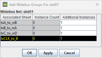
In this new widebus sheet, check the "Stat Mode" check box to reveal the AMI parameters
Update the layout as shown and detailed below.
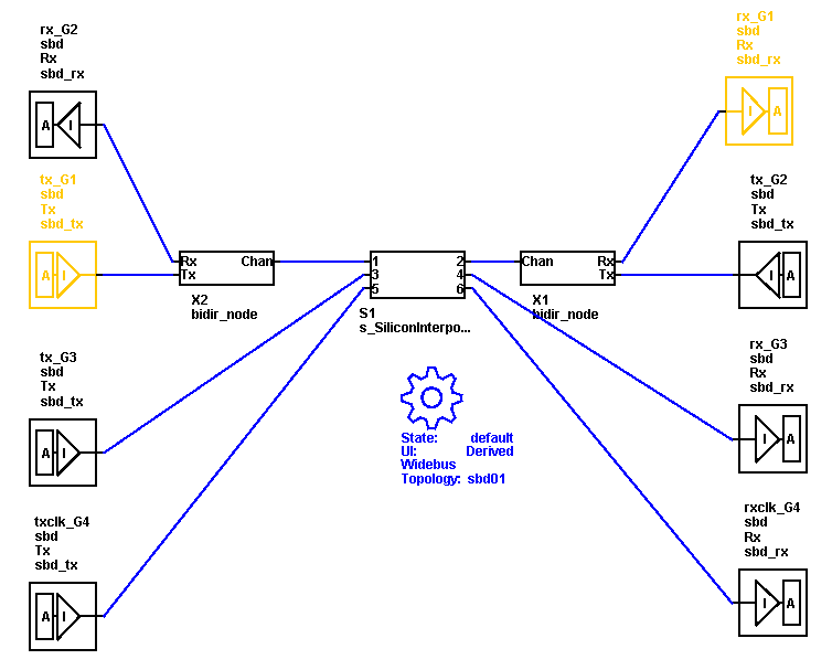
Add S-Parameter to sheet and browse to s_SiliconInterposerChannel01.s6p
Add an X sub-circuit to the canvas, then when asked to select a sub-circuit, browse to <Installation Library>/spice/connectors and select bidir_node.mod.
This block is essentially a three-way wire connection needed for joining the transmitter to the receiver on the same side.
Move tx_G2 to the right side and mirror it
Move rx_G2 to the left side and mirror it
Change the AMI model FileIndex values to facilitate the waveform file transfer between transmitters and receivers on the same die.
Select receiver "rx_G1" and identify the line in the Solution Space with a variable label of "rx_G1:EchoCancellation.FileIndex" and set it to "10".
Select transmitter "tx_G2" and identify the line in the Solution Space with a variable label of "tx_G2:ReplicaWriter.FileIndex" and set it to "10".
As we are only focusing on the right-side receiver for the SBD analysis, we can set the other FileIndex values in the solution space to unique integers to avoid conflicts. Select the following transmitters and set their FileIndex.
tx_G1 to 1
tx_G3 to 2
txclk_G4 to 3
There is a slight delay difference observed within the SBD receiver between the self-interference and the replica driver waveform. This is due to the channel reflection impulse response and needs to be compensated for. Future versions of the model will automatically configure this delay but we need to manually set it here.
Select the receiver "rx_G1" and find the variable "rx_G1:EchoCancellation.ReplicaDelay" and set this to "2.5e-12". If you are using your own S-Parameter, observe the unequalized impulse response found in the Statistical tab of the Signal Integrity Viewer after a simulation as shown below. Note that this response has a delay of about 2.5 ps.
Declare txCLK_to_B as a clock net. This is necessary to enable clock forwarding.
Right-click on any transmitter and select "Edit Transfer Nets"
For the txCLK_to_B sheet, change the type from Data to Clock
Change the stimulus patterns and define clock groups:
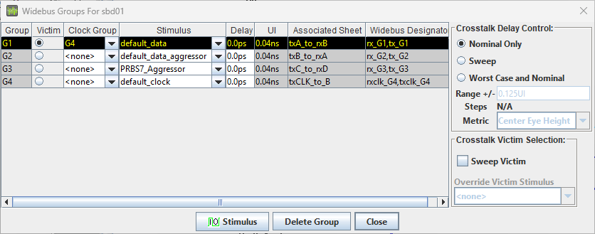
Double-click on a transmitter to open the Widebus Groups dialog
Change the stimulus patterns. Having different data patterns is important for the echo cancellation algorithm so that the desired signal and the interference signal data patterns are not correlated.
For G1 defined as the victim, select G4 as the clock group
In the Solution Space, select rxclk_G4 and ensure that rxclk_G4:Rx_Use_Clock_Input is set to None

In the Solution Space, select rx_G1 and set rx_G1:Rx_Use_Clock_Input to Wave. This will define the forwarded clock input of receiver G1 to accept the G4 net waveform. For this S-Parameter, we know the channel delay for all through paths is the same. Insert a 1/2 UI delay by setting the variable "rx_G1:DFEClkFwd.ForwardClockOffset" to 10 to ensure that the data and clock are properly aligned.

Set Simulation Parameters:
From the Prelayout Simulation dialog, click the Simulation Parameters... button
Change Rise Time to 10 ps
Uncheck Analyze Waveforms, Analyze Timing, and Display Results Spreadsheet
Select 'Simulation Options' and check 'skip standard load simulations'
After completing these steps, simulate the widebus sheet as described in the main workflow above. The results should match those shown in the "Run the Simulation and Interpret Results" section. If the simulation fails or produces unexpected results, see the Troubleshooting section.
See Also
Topics
- Simultaneous Bi-Directional Analysis in Simulink (SerDes Toolbox)

