Communications System with Embedded RF Receiver
This example shows how to integrate an RF receiver together with baseband signal processing algorithms to model an end-to-end communications system.
The example requires Communications Toolbox™.
Part 1: Baseband Communications Link with Integrated RF Receiver Model
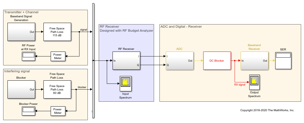
The following model includes a baseband signal generator, a simple channel, an RF receiver initially designed using the RF budget analyzer as described in Getting Started with RF Modeling, an analog-to-digital conversion, a demodulation scheme, and a computation block for the symbol error rate.
model = 'simrfV2_comms_rf_example';
open_system(model);

For this model, blocks from Communications Toolbox and DSP System Toolbox™ are used to perform baseband signal processing. The nonstandard compliant baseband signal has a rectangular QAM constellation with raised cosine filtering and the baseband receiver does not include carrier/clock synchronization. Parameters for the baseband signal generation are defined in the Model Properties -> Model callbacks PreLoadFcn, which sets these parameters in the MATLAB® workspace when the model is loaded:
BW = 8 MHz;
Tstep = 125 ns; % 1/BW
FrameLength = 128;
M = 4; % Constellation size 2^M
Tsymbol = 64 us; % M*FrameLength*Tstep
Sample time for the baseband signal and Step size of the RF Blockset™ receiver Configuration block have the same value. This guarantees that the RF simulation bandwidth is consistent with the sampling rate of the input signal. The RF Blockset Receiver has input and output ports that convert the Simulink® signals into RF domain quantities and scale their power to a 50 Ohm reference impedance. The input port centers the baseband signal at a specified center frequency of 2.45 GHz, and the RF IQ Demodulator downconverts the input signal to baseband with a single quadrature stage.
bdclose(model);
Part 2: Include an Out-of-Band Interfering Blocker Signal
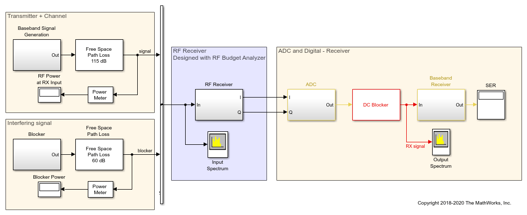
The model simrfV2_comms_rf_interferer shows how to add a high power out-of-band interferer centered around 2.5 GHz. This blocker affects the RF receiver by driving it into the nonlinear region. Use the following steps to complete this task.
model = 'simrfV2_comms_rf_interferer';
open_system(model);

Add an 8-PSK Modulator Baseband block source to include a blocking signal with a higher power level than the transmitter signal. Using the Vector Concatenate block, combine the baseband and blocker signals. The input signal to the RF receiver is now composed of two complex baseband signals. To ensure equal simulation bandwidths and maintain the same envelope bandwidth for each signal, it is crucial that the two baseband sources utilize the same sample rate. If the two signals don't have the same sample time, they need to be resampled before combining. This is the recommended best practice for simulating blocker signals when they are "far away" from the desired signal in the frequency spectrum and cannot be included in the same envelope for a particular carrier. To display the spectral positioning of the two input signals in the Spectrum Analyzer block, the Offset option has two frequencies specified for the two baseband signals.
The input port of the RF receiver has been modified to include the two carrier (Carrier frequencies) signals (2.45 GHz and 2.5 GHz). Initially we leave the configuration block to automatically select the fundamental tones and the harmonic order.
bdclose(model);
Part 3: Add Imperfections to the RF Receiver
The model simrfV2_comms_rf_impairments shows how to add impairments to the RF receiver that were initially not estimated in the link budget of the RF Budget Analyzer.
model = 'simrfV2_comms_rf_impairments';
open_system(model);

Under the mask of the RF receiver, modify the RF demodulator to add imperfections that will be driven by the blocking signal. In the mask of the IQ demodulator change these parameters:
I/Q gain mismatch= 0.5 dBI/Q phase mismatch= 1 degreeLO to RF isolation= 85 dBIIP2= 45 dBPhase noise frequency offset= [1e5 5e5 2e6] HzPhase noise level= [-95 -120 -140] dBc/Hz
Each of these imperfections separately increases the bit error rate. These imperfections cause finite image rejection and a DC offset that is removed in the baseband domain. As observed, the DC offset correction requires time to integrate the signal power and remove the DC component. To further modify the structure of the I/Q demodulator system, you can click on the "Edit System" button. With this operation you disable the link to the library, inline the value of the parameters, and have the ability to manually modify the block parameters as well as the block architecture.
bdclose(model);
Part 4: How to Decrease Simulation Time
The model simrfV2_comms_rf_speed shows how to decrease the simulation time of the previous model described in this example. Follow these steps to speed up the simulation of the model.
model = 'simrfV2_comms_rf_speed';
open_system(model);

In Simulink, select Accelerator mode to speed up the simulation by leveraging automatic C code generation.
In the RF Blockset section, to speed up simulation reduce the Harmonic order of the Circuit Envelope configuration block. Clear Automatically select fundamental tones and harmonic order and set the Harmonic order equal to 3. The Total simulation frequencies is reduced from 61 to 25, equivalent to an approximate 2.5 times speed up. After reducing the Harmonic order, verify that simulation results do not change.
To further increase simulation speed, use Frequency domain modeling instead of Time domain modeling for the S-parameters SAW filter block. You need to verify that when changing the Compare Time and Frequency Domain Simulation Options for S-parameters approach the simulated transfer function is still correct and that the model uses a sufficiently long Impulse response duration.
With the above modifications, the simulation is approximately five times faster without significantly affecting the simulation results.
bdclose(model);
clear model;