Main Content

Memory IIO Write

Write from simulation model to a shared memory region

Since R2023a

Add-On Required: This feature requires the SoC Blockset Support Package for AMD FPGA and SoC Devices add-on.

  • Memory IIO Write block

Libraries:
SoC Blockset Support Package for AMD FPGA and SoC Devices / Common / Host I/O

Description

The Memory IIO Write block performs random-access write transactions to DDR memory in the connected Xilinx® SoC device from a Simulink® model running on the host computer. This block enables low-latency high-throughput data transmission between your simulation model and the DDR memory on the SoC device.

The Memory IIO Write block sends data to the DDR memory on the SoC device from the host computer. This block uses the Industrial I/O (IIO) library driver to create a network server daemon on the SoC device and client host computer to pass the data from the host computer running the simulated portion of the model. This diagram shows the connection between the FPGA, DDR memory, and communication bridge to the Simulink model.

Memory IIO Write diagram

Ports

Input

expand all

This port receives the data vector that it writes to the memory.

Data Types: single | double | int8 | int16 | int32 | int64 | uint8 | uint16 | uint32 | uint64 | ufix128

The offset of the memory address from the base address of the IP core on the device. The block writes data to this address.

Dependencies

To enable this port, select Enable address offset port.

Data Types: single | double | int8 | int16 | int32 | int64 | uint8 | uint16 | uint32 | uint64 | ufix128

Parameters

expand all

Enter the name and channel of the IP core on the FPGA as a colon-separated list.

Note

If you are using HDL Coder™ to generate the IP core, HDL Coder maps the IP core to mwipcore0 and uses channel sharedmem0:wr0.

Select this parameter to use the address offset from a port.

  • On — The Address offset parameter is disabled, and an addr input port is created.

  • Off — The Address offset parameter is enabled.

Enter the offset of the memory from the base address of the IP core on the device. The block reads data from this address.

Note

If you use HDL Coder to generate the IP core, you can get the value of the address offset from the “Register Address Mapping” section of Custom IP Core Report (HDL Coder). For more information, see Register Address Mapping (HDL Coder).

Dependencies

To enable this parameter, clear the Enable address offset port parameter.

Enter the network address of the connected SoC device.

Example: 10.0.0.201

Specify the maximum timeout delay for the memory write.

When the host computer is connected to a board and this parameter is on, this block writes data directly to the board. When you use this parameter in a simulation environment, clear the parameter to enable simulation without error due to lack of IIO connection. When you clear this parameter, the data that the data output port displays does not reflect actual data.

Tips

To get a list of available IIO device names and channels, open a terminal to the Xilinx Zynq® device and execute this command: iio_info. This display shows the sample output from the iio_info command.
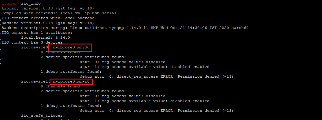
command line info from iio_info

Version History

Introduced in R2023a