Custom IP Core Report
R2026bYou generate an HTML custom IP core report by default when you generate a custom IP core. The report describes the behavior and contents of the generated custom IP core.
Summary
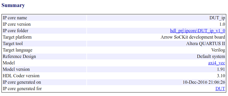
The Summary section shows your coder settings when you generated the custom IP core.
The following figure is an example of a Summary section.
Target Interface Configuration
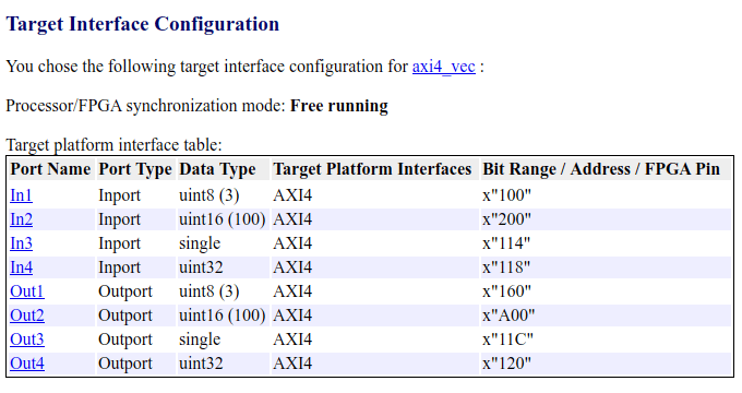
The Target Interface Configuration section shows how your DUT ports map to the target hardware interface and the processor/FPGA synchronization mode.
The following figure is an example of a Target Interface Configuration section.
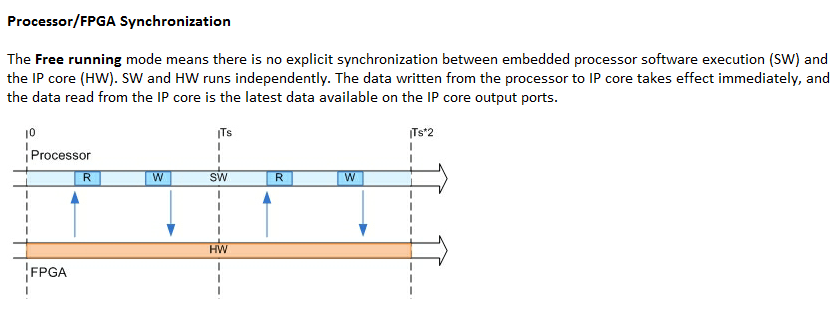
To learn more about processor/FPGA synchronization modes, see Processor and FPGA Synchronization.
To learn more about target platform interfaces, see Custom IP Core Generation.
Register Address Mapping
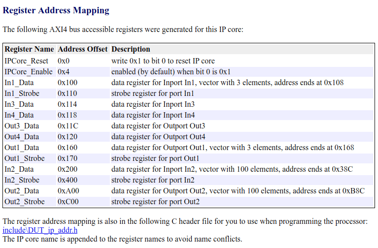
The Register Address Mapping section shows the address offsets for AXI4-Lite bus accessible registers in your custom IP core, and the name of the C header file that contains the same address offsets.
The following figure is an example of a Register Address Mapping section.
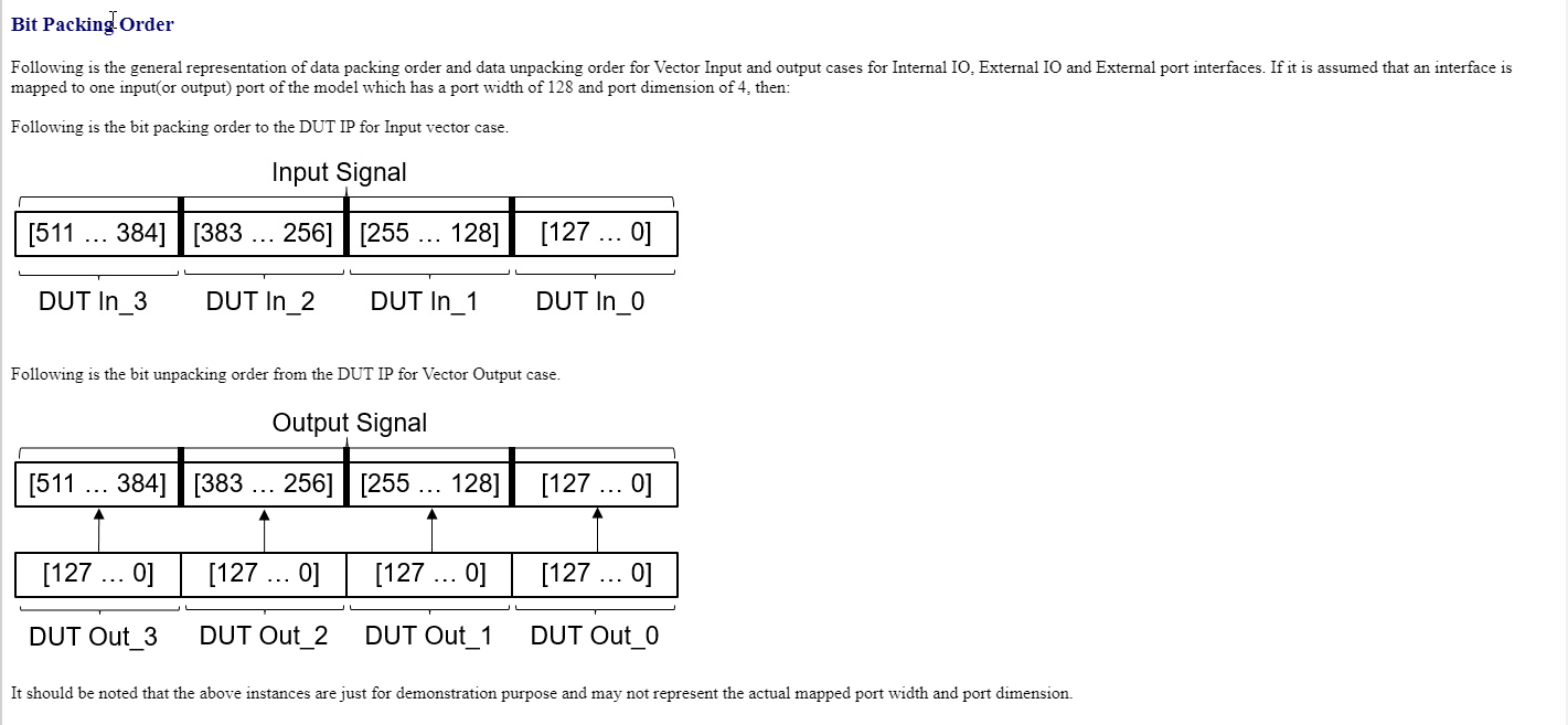
Bit Packing Order
The Bit Packing Order section gives a high-level overview of the data packing order for vector inputs and outputs for Internal IO, External IO, and External port interfaces. This section only appears when the port width for Internal IO, External IO, and External ports are set to greater than 128 bits wide.
This image is an example of the Bit packing Order section:
IP Core User Guide
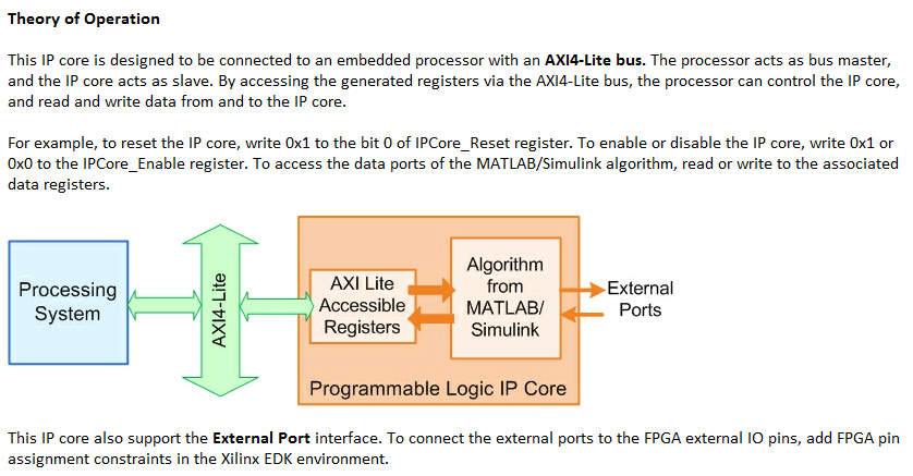
The IP Core User Guide section gives a high-level overview of the system architecture, describes the processor and FPGA synchronization mode, and gives instructions for integrating the IP core in your embedded system integration environment.
The following figure is an example of an IP Core User Guide system architecture description.
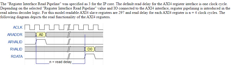
When your design under test (DUT) contains any register, HDL Coder™ add this section to the IP core generation report:
The following figure is an example of a processor/FPGA synchronization description.
If you use vector data signals at the DUT interface, the IP core report displays this section that shows how the code generator synchronizes vector data across the AXI4 interface.
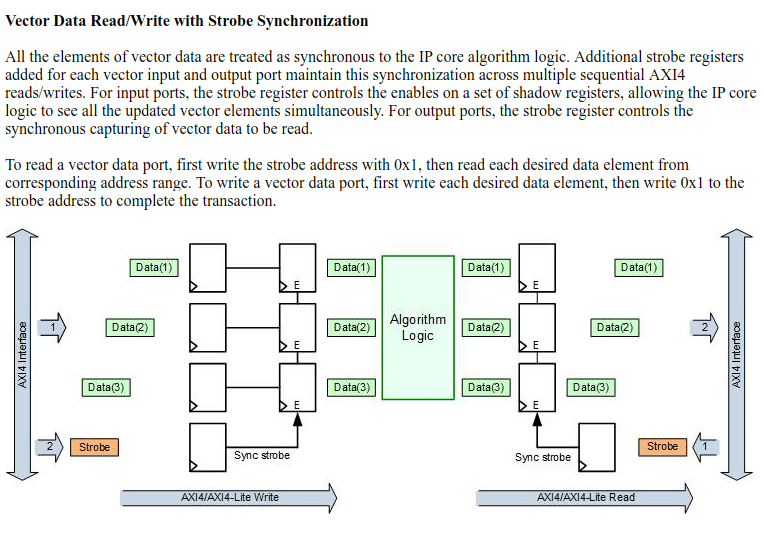
The following figure is an example of instructions for integrating the IP core into your embedded system integration environment on the Xilinx® platform. If you are targeting an Altera® platform, the report displays similar instructions for integrating the IP core into the Altera Qsys environment.
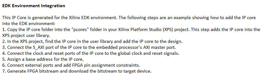
IP Core File List
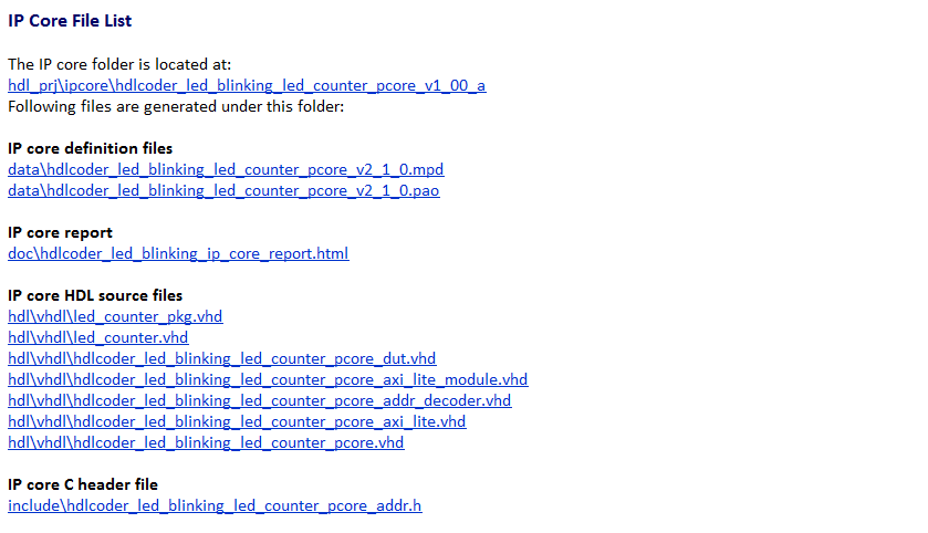
The IP Core File List section lists the files and file folders that comprise your custom IP core.
The following figure is an example of an IP core file list.
Frame-to-Sample Mode
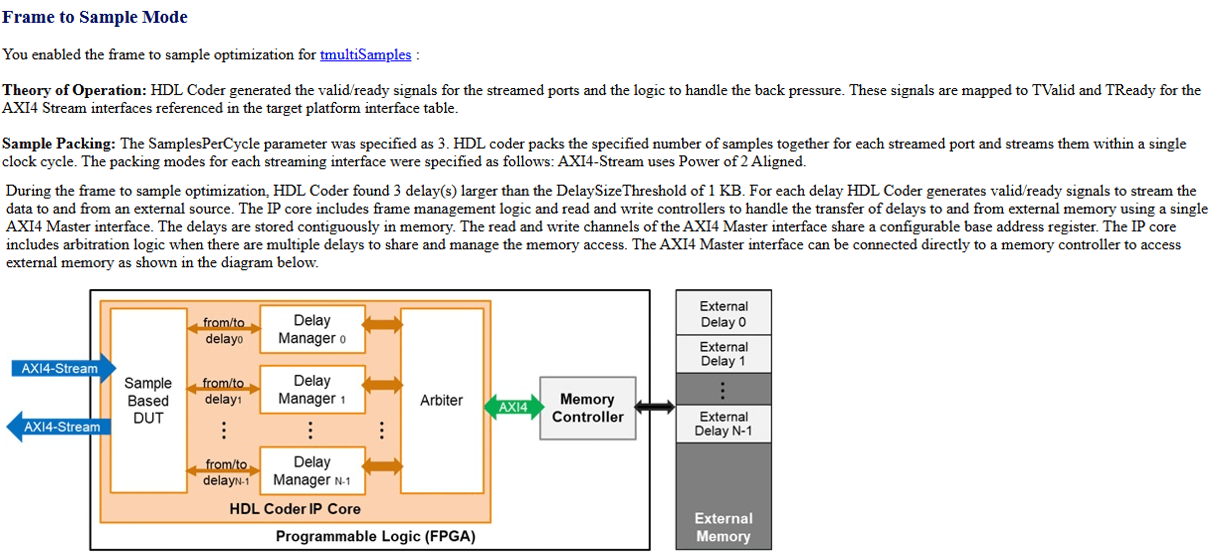
When you enable the frame-to-sample optimization, the IP core report includes a Frame-to-Sample Mode section, which includes the Frame-to-Sample Mode section, which includes information such as high-level overviews of the frame-to-sample optimization, the generated code, and a summary of how the data is packed and streamed.
This image shows the section of the Frame-to-Sample Mode section, which includes an overview of the theory of operation for the frame-to-sample optimized IP core and a summary of how the large delays are offloaded to external memory.
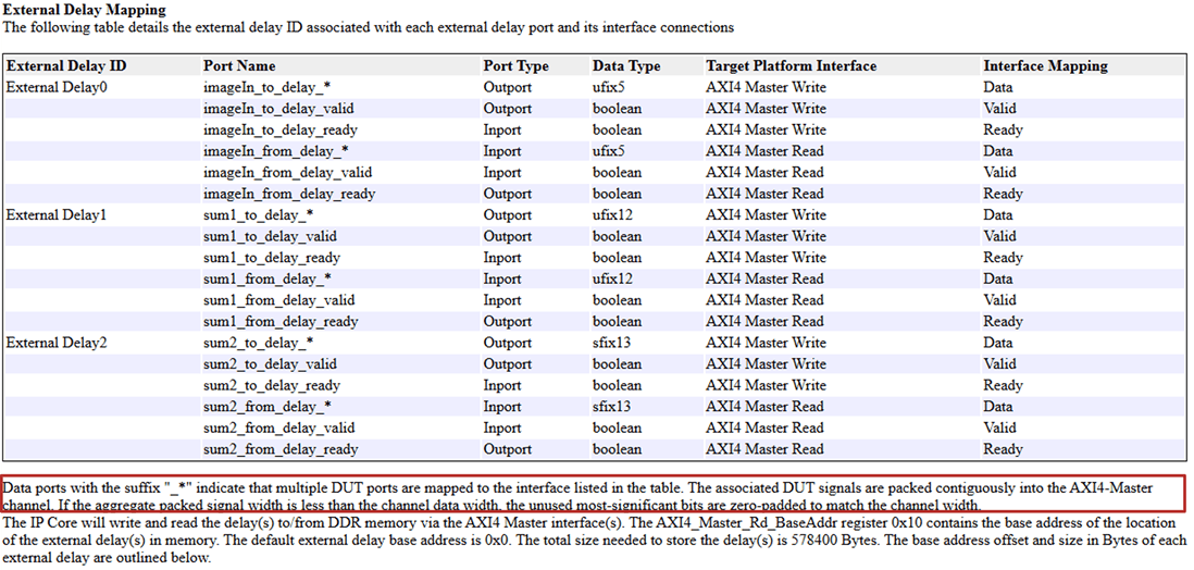
When the design has implicit delays or design delays that exceed a specified
threshold, the report includes the External Delay Mapping section, which details
information about the external delay mapping such as delay ID, port name, AXI4-Master
interfaces, and so on. This image shows the interface mapping table and in the table
Port names with an * next to the name indicate that multiple signals
are mapped to that port.
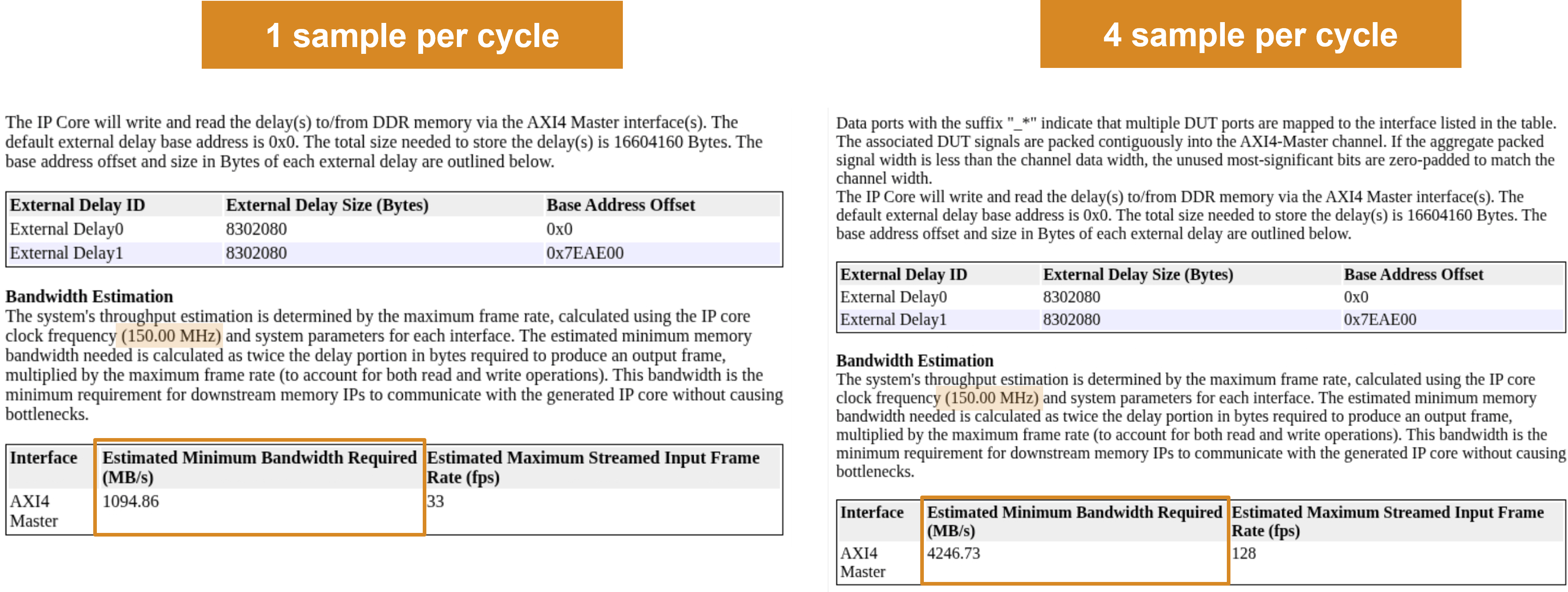
This image shows the delay mapping and bandwidth estimation portion of the report. The bandwidth calculations include the updated multiple samples per cycle value.