生成 IP 核和比特流
R2026a生成 HDL IP 核和比特流,包含用于部署在独立 FPGA 板、Speedgoat® I/O 模块、Xilinx® Zynq®-7000 平台、Intel® SoC 器件或 Microchip SoC 器件上的 HDL 代码
IP 核是实现特定函数(通常是算法)的可共享和可重用 HDL 组件。一个 IP 核包含 IP 核定义文件、为算法生成的 HDL 代码、包含寄存器地址映射的 C 头文件和 IP 核报告。
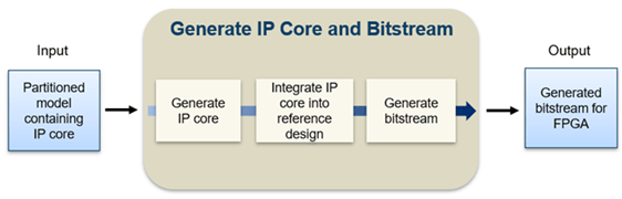
通过使用 HDL 工作流顾问中的 IP Core Generation 工作流,HDL Coder™ 可以生成一个 IP 核(其中包含 HDL 源代码和用于将 IP 核集成到 Vivado®、Qsys 或 Libero® 工程中的 C 头文件),然后对目标硬件进行编程。您可以根据目标平台将 IP 核集成到默认或自定义参考设计中,并生成要部署到 FPGA 硬件的比特流。输入是 Simulink® 模型或 MATLAB® 函数中设计的 IP 核。输出是由 HDL Coder 从 IP 核生成的比特流。
有关工作流的更多详细信息,请参阅Targeting FPGA and SoC Hardware Overview。
类
hdlcoder.WorkflowConfig | Configure HDL code generation and deployment workflows |
主题
IP 核生成
- Custom IP Core Generation
Generate a custom IP core from a model or algorithm using the HDL Workflow Advisor. - Custom IP Core Report
You generate an HTML custom IP core report by default when you generate a custom IP core. - Generate Board-Independent HDL IP Core from Simulink Model
When you open the HDL Workflow Advisor and run theIP Core Generationworkflow for your Simulink model, you can specify a generic Xilinx platform, a generic Intel platform, generic Microchip platform or generic platform. - Generate Board-Independent IP Core from MATLAB Algorithm
Board-independent IP core generation from MATLAB. - Generate HDL IP Core with Multiple AXI4-Stream and AXI4 Master Interfaces
Learn how you can map your DUT ports to multiple AXI4-Stream, AXI4-Stream Video, and AXI4 Master interfaces. - IP Core Reset Interface
Learn how HDL Coder automatically inserts logic to synchronize global reset signal to IP core clock domain. - IP Core Generation Workflow for Standalone FPGA Devices
Learn how to use the IP Core Generation workflow with standalone FPGA devices and embed the IP core into the reference design. - Generate Board-Independent HDL IP Core for Xilinx Platforms
Integrate generated IP core into a AMD® Vivado project. (自 R2024b 起)
Xilinx Zynq 参考设计
Intel SoC 参考设计
- Default System Reference Design for Altera SoC Devices
Learn about the default system reference design and using the reference design for Altera® SoC Devices. - Default System with External DDR4 Memory Access Reference Design
Learn about the default system with external DDR3 memory access reference design and its requirements.
Microchip SoC 参考设计
- Default System Reference Design
Learn about the default system reference design and using the reference design.
参考设计集成
- IP Caching for Faster Reference Design Synthesis
Use IP caching to speed up reference design synthesis time by using an out-of-context workflow. - Resolve Timing Failures in IP Core Generation and Simulink Real-Time FPGA I/O Workflows
Resolve timing failures in Build FPGA Bitstream step of IP Core Generation Workflow or Simulink Real-Time FPGA I/O Workflow for Vivado-Based Boards.
精选示例
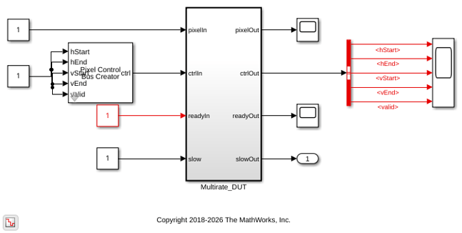
Generate IP Core from Multirate Model
Learn various example designs that use multiple sample rates with IP Core Generation workflow.
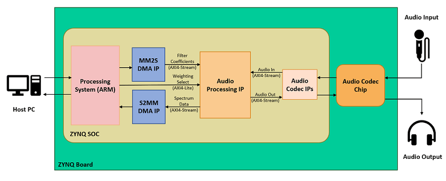
Generate IP Core with Multiple AXI4-Stream Channels
Model an audio system with multiple AXI4-Stream channels and deploy it on a ZedBoard™ by using an audio reference design.
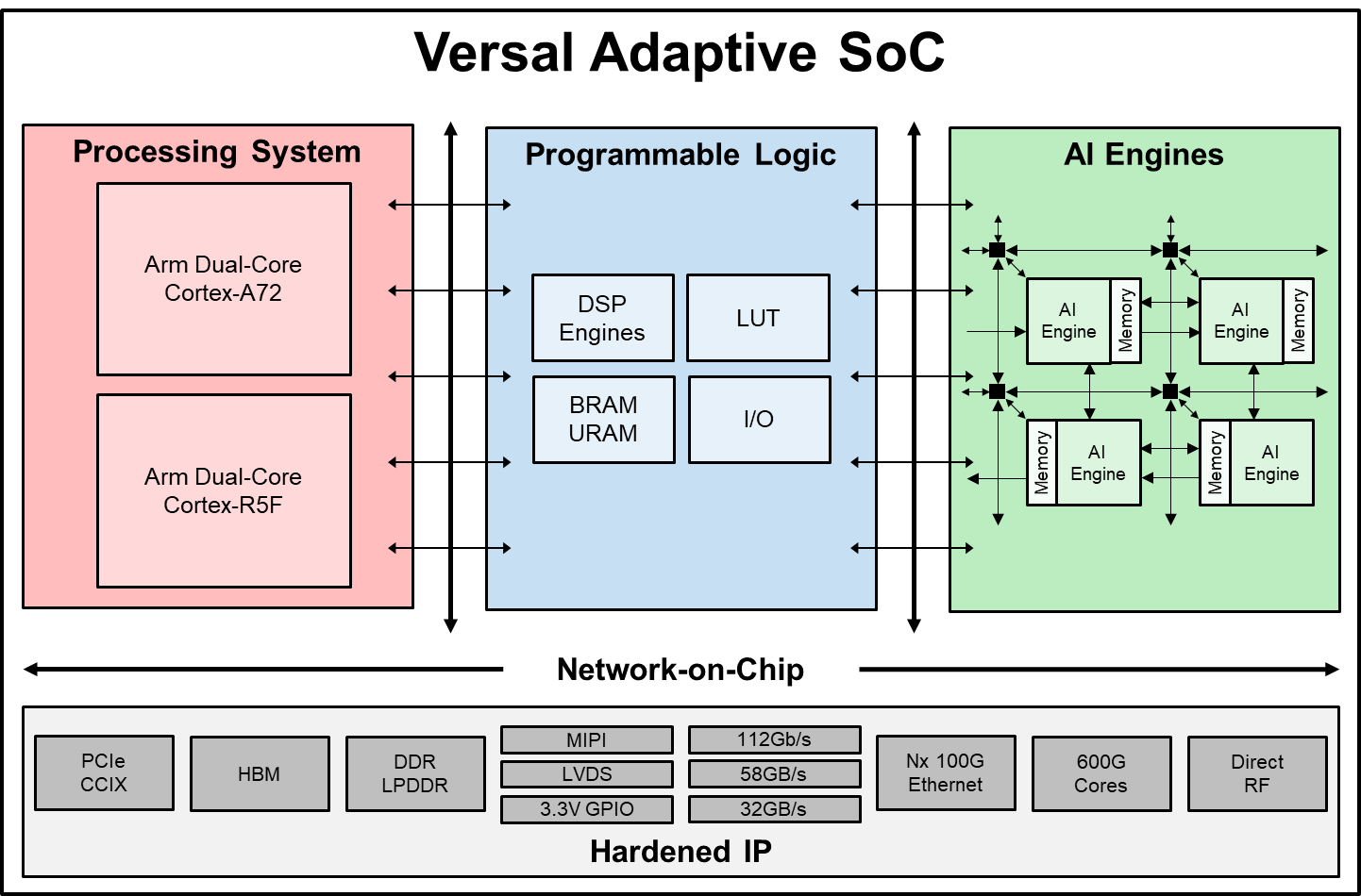
Integrate HDL IP Core with Versal AI Engine
Model, partition, and deploy a design that leverages the processor, FPGA, and AI Engines on a Versal device.

