Operational Transconductance Amplifier
Behavioral representation of operational transconductance amplifier
Libraries:
Simscape /
Electrical /
Integrated Circuits
Description
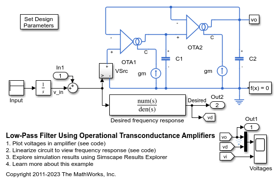
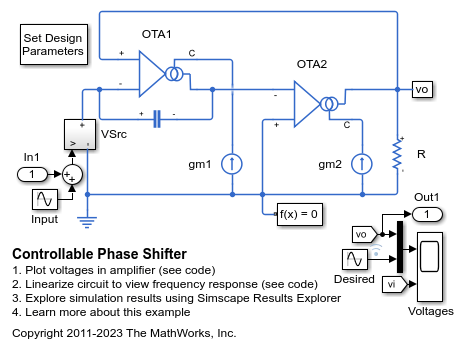
The Operational Transconductance Amplifier block provides a behavioral representation of an operational transconductance amplifier. A transconductance amplifier converts an input voltage into an output current. Applications include variable frequency oscillators, variable gain amplifiers and current-controlled filters. These applications exploit the fact that the transconductance gain is a function of current flowing into the control current pin.
To support faster simulation, the behavioral representation does not model the detailed transistor implementation. Therefore, the model is only valid when operating in the linear region, that is, where the device input resistance, output resistance, and transconductance gain all depend linearly on the control current, and are independent of input signal amplitude. The dynamics are approximated by a first-order lag, based on the value you specify for the block parameter Bandwidth.
Control Current
The control current pin C is maintained at the voltage that you
specify for the Minimum output voltage. In practice, the
Minimum output voltage equals the negative supply
voltage plus the transistor collector-emitter voltage drop. For example, if the
Minimum output voltage for a supply voltage of +-15V
is -14.5, then to achieve a control current of 500μA, a resistor connected between
the +15V rail and the control current pin must have a value of (15 - (-14.5)) /
500e-6 = 59kOhm.
Transconductance
The relationship between input voltage, v, and transconductance current, igm, is:
where:
v+ is the voltage presented at the block
+pin.v– is the voltage presented at the block
-pin.gm is the transconductance.
ic is the control current flowing into the control current pin
C.ic0 is the reference control current, that is, the control current at which transconductance is quoted on the datasheet.
gm0 is the transconductance measured at the reference control current ic0.
Therefore, increasing control current increases the transconductance.
Output Resistance and Determining Output Current
The output resistance, Rout, is defined by:
where:
igm is the transconductance current.
io is the output current, defined as positive if flowing into the transconductance amplifier output pin.
ic is the control current flowing into the control current pin
C.ic0 is the reference control current, that is, the control current at which output resistance is quoted on the datasheet.
Rout0 is the output resistance measured at the reference control current ic0.
Therefore, increasing control current reduces output resistance.
Input Resistance
The relationship between input voltage, v, across the
+ and - pins and the current flowing,
i, is:
where:
ic is the control current flowing into the control current pin
C.Rin is the input resistance for the current control current value, ic.
ic0 is the reference control current, that is, the control current at which input resistance is quoted on the datasheet.
Rin0 is the input resistance measured at the reference control current ic0.
Therefore, increasing control current reduces input resistance.
Limits
Because of the physical construction of an operational transconductance amplifier based on current mirrors, the transconductance current igm cannot exceed the control current. Hence the value of igm is limited by:
| –ic ≤ igm ≤ ic | (1) |
The output voltage is also limited by the supply voltage:
| Vmin ≤ vo ≤ Vmax | (2) |
where Vmin is the Minimum output voltage, and Vmax is the Maximum output voltage. Output voltage limiting is implemented by adding a low resistance to the output when the voltage limit is exceeded. The value of this resistance is set by the Additional output resistance at voltage swing limits parameter.
The transconductance current is also slew-rate limited, a value for slew rate limiting typically being given on datasheets:
where μ is the Maximum current slew rate.
Examples
Ports
Conserving
Parameters
Extended Capabilities
Version History
Introduced in R2011b


