SPICE NIGBT
SPICE-compatible N-Channel insulated gate bipolar transistor

Libraries:
Simscape /
Electrical /
Additional Components /
SPICE Semiconductors
Description
The SPICE NIGBT block models a SPICE n-type insulated gate bipolar transistor (IGBT).
SPICE, or Simulation Program with Integrated Circuit Emphasis,
is a simulation tool for electronic circuits. You can convert some SPICE subcircuits into
equivalent Simscape™
Electrical™ models using the Environment Parameters block and
SPICE-compatible blocks from the Additional Components library. For more
information, see subcircuit2ssc.
This figure shows the equivalent circuit for the SPICE NIGBT block:
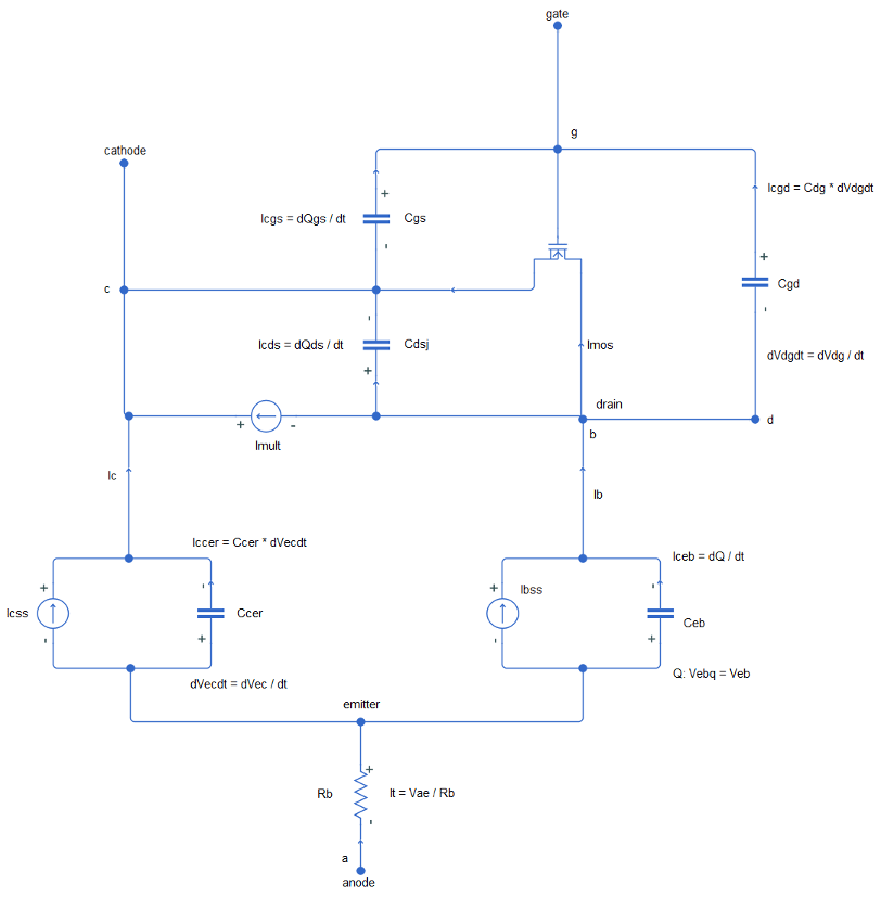
Equations
Variables for the SPICE NIGBT block equations include:
Variables that you define by specifying parameters for the SPICE NIGBT block.
Temperature, T, which is
300.15Kby default. You can use a different value by specifying parameters for the SPICE NIGBT block or by specifying parameters for both the SPICE NIGBT block and an Environment Parameters block. For more information, see Transistor Temperature.
This table shows the equations that define the relationship between the MOSFET channel current, Imos, and the gate-source voltage, Vgs.
| Applicable Range of Vgs Values | Corresponding Imos Equation |
|---|---|
In these equations:
Vds is the drain-source voltage.
VT is the threshold voltage.
KF is the triode region factor.
KP is the mosfet transconductance.
THETA is the transverse field factor.
This table shows the equations that define the relationship between the steady-state collector current, Icss, and the emitter-base capacitance, Qeb.
| Applicable Range of Qeb Values | Corresponding Icss Equation |
|---|---|
In these equations:
is the ambipolar mobility ratio.
is the diffusion coefficient for holes.
is the quasi-neutral base width, where:
WB is the metallurgical base width.
is the base-collector depletion width.
Vbc is the base-collector voltage.
Vbi is the built-in voltage, and it is equal to
0.6V
This table shows the equations that define the relationship between the steady-state base current, Ibss, and the emitter-base capacitance, Qeb.
| Applicable Range of Qeb Values | Corresponding Ibss Equation |
|---|---|
In these equations:
TAU is the ambipolar recombination lifetime.
JSNE is the emitter saturation current density.
ni is the intrinsic carrier concentration. At
300Kit is equal to1.45*10101/cm3.is the background mobile carrier base charge, where:
NB is the base doping.
AREA is the area of the device.
This table shows the equations that define the relationship between the emitter-base voltage, Veb, and the emitter-base capacitance, Qeb.
| Applicable Range of Qeb Values | Corresponding Veb Equation |
|---|---|
In these equations:
is the emitter-base depletion voltage.
Vbi is the built-in voltage.
is the emitter-base junction built-in voltage.
is the emitter-base diffusion voltage.
The anode current is obtained from this equation:
where:
Vae is the applied anode-emitter voltage.
Rb is the conductivity-modulated base resistance.
This table shows the equations that define the relationship between the conductivity-modulated base resistance, Rb, and the emitter-base capacitance, Qeb.
| Applicable Range of Qeb Values | Corresponding Rb Equation |
|---|---|
In these equations:
μeff is the effective carrier mobility.
neff is the effective base doping concentration.
MUN is the electron mobility.
μeff and neff are obtained using these equations:
where:
μnc is the electron carrier scattering mobility.
μpc is the hole carrier scattering mobility.
Dc is the carrier-carrier scattering diffusivity.
L is the ambipolar diffusion length.
P0 is the carrier concentration at emitter's end of the base.
is the average carrier concentration in base.
The avalanche multiplication current is obtained from this equation:
where:
is the collector-base thermally generated current.
Icss is the steady-state collector current.
Imos is the MOSFET channel current.
Iccer is the collector-emitter redistribution current.
This equation defines the relationship between the base-collector voltage, Vbc, and the avalanche multiplication factor, M:
where:
is the open-base collector-emitter breakdown voltage.
BVF is the avalanche uniformity factor.
BVN is the avalanche multiplication exponent.
The gate source capacitance is obtained from this equation:
The drain source capacitance is obtained from this equation:
where Wdsj = Wbcj is the drain-source depletion width.
This table shows the equations that define the relationship between the gate-drain capacitance, Qdg, and the drain-gate voltage, Vdg
| Applicable Range of Vdg Values | Corresponding Qdg Equation |
|---|---|
In these equations:
is the gate-drain overlap oxide capacitance.
Vdg is the drain-gate voltage.
εsi is the permittivity of silicon.
is the drain-gate overlap depletion width.
VTD is the Gate-drain overlap depletion threshold, VTD.
COXD is the Gate-drain oxide capacitance per unit area, COXD.
AGD is the Gate-drain overlap area, AGD.
NB is the Base doping, NB.
This equation shows the relationship between the collector-emitter redistribution current, Iccer, and the collector-emitter redistribution capacitance, Ccer:
where Vec is the emitter-collector voltage.
This table shows the equations that define the relationship between the collector-emitter redistribution capacitance, Ccer, and the emitter-base capacitance, Qeb.
| Applicable Range of Qeb Values | Corresponding Ccer Equation |
|---|---|
In these equations:
Cbcj is the base-collector depletion capacitance.
is the background mobile carrier base charge.
The implicit emitter-base capacitor current is obtained from this equation:
You can use these options to define transistor temperature, T:
Fixed temperature — The block uses a temperature that is independent of the circuit temperature when the Model temperature dependence using parameter in the Temperature settings of the SPICE NIGBT block is set to
Fixed temperature. For this model, the block sets T equal to TFIXED.Device temperature — The block uses a temperature that depends on circuit temperature when the Model temperature dependence using parameter in the Temperature settings of the SPICE NIGBT block is set to
Device
									temperature
. For this model, the block defines temperature aswhere:
TC is the circuit temperature.
If there is not an Environment Parameters block in the circuit, TC is equal to 300.15 K.
If there is an Environment Parameters block in the circuit, TC is equal to the value that you specify for the Temperature parameter in the SPICE settings of the Environment Parameters block. The default value for the Temperature parameter is
300.15K.TOFFSET is the offset local circuit temperature.
Ports
Refer to the figure for port locations.
![]()
Conserving
Parameters
References
[1] Hefner, A.R. and Diebolt, D.M. An experimentally verified IGBT model implemented in the Saber circuit simulator. IEEE transactions on Power Electronics 9, no. 5 (September 1994): 532-42. https://doi.org/10.1109/63.321038.
[2] Hefner, A.R., Jr. Semiconductor measurement technology: INSTANT - IGBT Network Simulation and Transient ANalysis Tool. U.S. Department of Commerce/Technology Administration, National Institute of Standards and Technology. 1992.
Extended Capabilities
Version History
Introduced in R2020a