Three-Phase High-Power Converter Design and Analysis Workflow
This example shows the main steps involved in designing a high-power converter. High power converters are important building blocks for future electric mobility and microgrid solutions. To design a cost effective, lightweight, efficient converter, you must perform detailed analysis of different converter design options and deployment scenarios. This example helps you to simulate the steady state, transient electrical, and thermal characteristics of a three-phase two-level converter that uses Insulated-Gate Bipolar Transistor (IGBT) devices.
Converter Design and Analysis Workflow
This flowchart shows how to perform a converter analysis and how to study the effects of design decisions and component parameters. This analysis allows you to find an efficient and cost-effective design.

The N-Channel IGBT and Diode blocks of this example are parameterized to correctly captures the on-state losses and the switching losses. The Modeling option parameter of the N-Channel IGBT block is set to Full I-V and capacitance characteristics. The Diode model parameter of the Diode block is set to Tabulated I-V curve. The characteristics curves in the manufacturer datasheet provide the parameters for these blocks.
If you want to use this example for other IGBT and Diode devices, to carry out the trade-off studies and design optimization, you must provide proper parameterized data that is efficient to simulate.
The ConverterDesignIGBTDatasheetParameters MAT file contains the parameterized data for the N-Channel IGBT, Diode, Heatsink, and IGBT(Ideal, Switching) blocks. To load the device parameters in the workspace, at the MATLAB Command Window, enter:
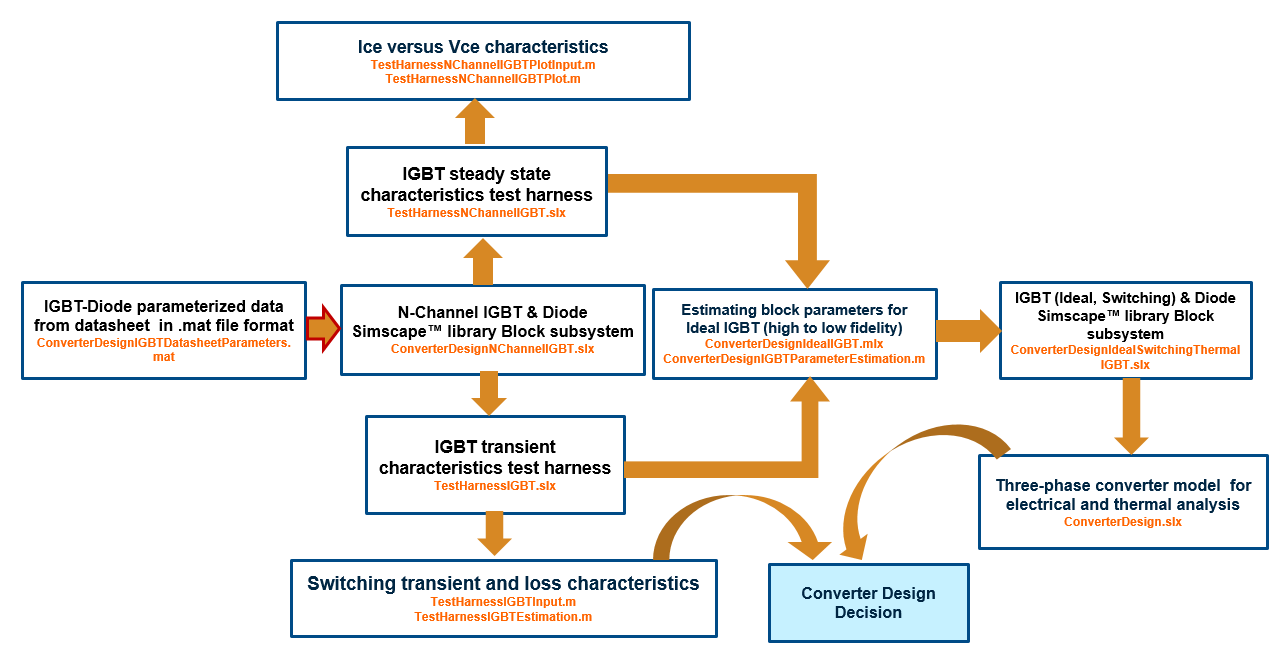
High-Power Converter Design Data Flow Diagram
This figure shows the data flow and the respective file names used in this example.
Select the IGBT Device
This example is based on a 15 kW converter that operates in a three-phase grid with frequency of 60Hz and line voltage of 208 V. The RMS current of the converter is equal to 15e3/(sqrt(3)*208) = 41.6 Amperes and the current peak is equal to 59 Amperes. Because the minimum required DC bus voltage is equal to 2*208*sqrt(2/3) = 340 Volts, this example chooses a standard 400V DC bus.
Due to the required currents and voltage, the converter needs an IGBT rated at more than 450Vdc and 50A. The TO-247 package contains an IGBT device with a continuous current rating of 50 Amperes and 650 Volts rating. The parasitic inductance of the busbar that connects the IGBT device with the DC bus is assumed to be 30nH. The busbar inductance is calculated either through lab measurement or by 3-D electromagnetic simulation.
Extract IGBT Parameters
IGBT devices are the most used semiconductor switches for high-power inverters thanks to their unique ability of better switching frequency, simpler gate driver, and available power rating. The N-Channel IGBT and the IGBT (Ideal, Switching) blocks in the Simscape™ Electrical™ library both model an IGBT device. The two blocks provide support for different modeling fidelity levels. The IGBT (Ideal, Switching) block is more suited to system-level simulations. The N-Channel IGBT block is more suited to detailed designs, such as gate driver design and simulating peak switching voltage and current.
N-Channel IGBT Block Overview
The N-Channel IGBT block provides a detailed model of an IGBT device by supporting the definition of non-linear I-V characteristics, either through physical equations or by lookup tables. It also supports the definition of nonlinear charge characteristics either through simple physical equations or lookup tables. The block parameterization matches the data in the manufacturer datasheet. The datasheet information usually includes:
 at two different junction temperatures.
Capacitance
 as a function of
  .
.Diode
 as a function of
  for two junction temperatures.
Parameters for thermal model (Foster, Cauer, or simple
 ).
).Switching loss curves
 and
and 
You can create the necessary tabulated data for the block from the datasheet characteristic plots. You can perform a more approximate parameterization by using the datasheet tabulated values only. Note that many datasheets only provide the  versus
  data for the
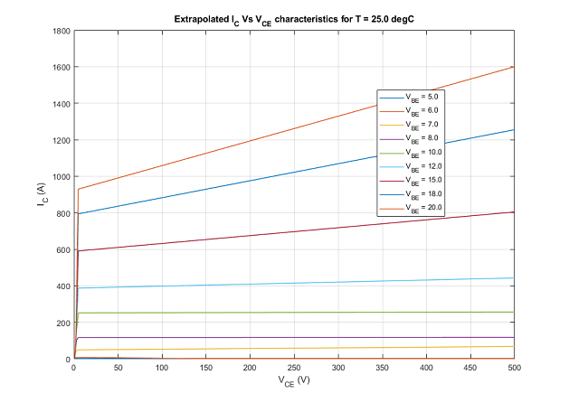
  up to 5V, but a switching IGBT device goes through a transition from 0V to the DC bus voltage. In these cases, to avoid extrapolation to non-physical current values, provide some estimated values at higher voltage ranges.
In converters, an IGBT device operates in switching mode. For good simulation speed and accuracy, you must ensure accurate and smooth  values around the smaller collector-emitter voltages.
This plot shows the extension of the datasheet data to include points at the DC bus voltage for the device in this example.
% This plot shows the digitalized device capacitance characteristics.

This plot shows the external diode forward current characteristics  , obtained from the IGBT datasheet.

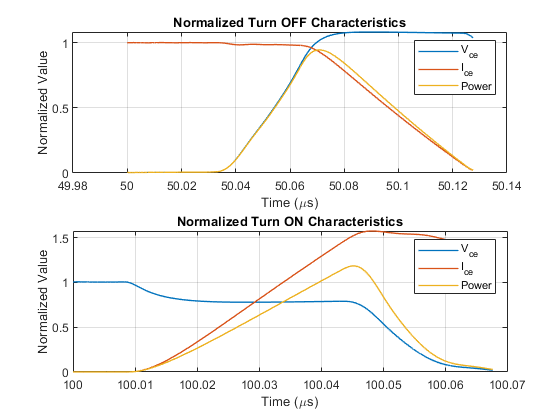
Simulated Switching Transient
This figure shows the simulated N-Channel IGBT switching turn-on and turn-off characteristics.
IGBT (Ideal, Switching) Library Block
The detailed N-Channel IGBT block requires very low simulation time steps to capture the turn-on and turn-off transients. This slows down the simulation too much when this block is used in large models. To improve the simulation speed, you can use the IGBT(Ideal, Switching) block. This is ideal when you are looking at system-level harmonics or thermal simulation including heat sink dynamics and cooling. The IGBT(Ideal, Switching) block implements instantaneous junction temperature changes due to conduction, turn-on and turn-off losses.
N-Channel IGBT Device Model Subsystem
A Subsystem Reference model contains the parameterized N-Channel IGBT block. Use this subsystem to define the block once and then use it in multiple models. The Subsystem Reference includes the terminal lead parasitic inductance.

Design the Gate Driver
Simscape Electrical also helps you to design a gate driver circuit for controlling power electronics devices. This example models three gate drivers to switch semiconductor devices.
Ideal Gate Driver
An ideal gate driver models the charging gate resistance and the discharging gate resistance and provides flexibility to define the turn-on and turn-off gate voltages  .
.

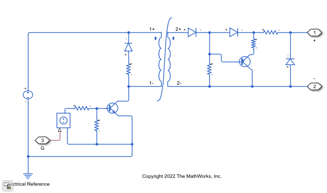
Gate Driver with Galvanic Isolation (Pulse Transformer)
A gate driver with galvanic isolation is a high frequency transformer-based gate driver that requires only a single gate driver power supply. This supply is isolated from the power circuit.
To simulate the gate driver with electromagnetic isolation with the N-Channel IGBT block, open the TestHarnessIGBT SLX model and, in the masked selection subsystem in the top-right corner, choose Gate driver with electromagnetic isolation.
Gate Driver with Opto-Coupler Isolation
A gate driver with optocoupler isolation is a compact gate driver with lower losses. This gate driver requires two gate driver power supplies that are isolated from each other and from the power circuit.
To simulate the gate driver with optocoupler isolation with the N-Channel IGBT block, open the TestHarnessIGBT SLX model and, in the masked selection subsystem in the top-right corner, choose Gate driver with opto-coupler.

Test Harness for IGBT Steady State Characteristics
The TestHarnessNChannelIGBT SLX model provides test harness to plot the steady state  curve for different junction temperature
  and gate-emitter voltage
  .
.

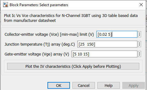
IGBT Steady State Characteristics Test Harness Parameter Selection Mask
To define simulation parameters, in the TestHarnessNChannelIGBT SLX model, open the "Specify Test Parameters" mask in the top right corner. Then click on the "Plot iv-characteristics" button to get the required i-v characteristics curve.
Test Harness for High-Power Converter Switching Loss Estimation
The model TestHarnessIGBT, provides test harness that plots the variation of switching loss characteristics for these IGBT simulation parameters:
Collector-emitter current

PWM switching frequency

Gate-emitter voltage

Collector-emitter voltage

Gate resistance

Junction temperature

This model plots the IGBT characteristics for both double pulse and sinusoidal PWM gate signals. The IGBT device under test is placed in the lower (IGBTL) leg of a converter. A double pulse gate signal is used to determine the single turn-on and turn-off characteristics. A sinusoidal PWM gate modulation signal is used along with a sinusoidal output collector current to simulate the voltage  and current
  stress on the IGBT-diode device combination in a typical two-level converter. A sinusoidal output load current with sinusoidal voltage modulation signal enables you to simulate for different power factor, power frequency, and switching frequency.
In the two-level converter, when bottom IGBT device is turned-on, the conduction transfer from top diode to bottom IGBT and vice versa during IGBT-turn-off. Busbar inductance influence the turn-off switching loss, it creates off state voltage spike across the device. Diode reserve recovery current affects the IGBT turn-on characteristics. It creates on-state current spike through the device.

Switching Loss Estimation Test Harness Parameter Selection Mask
To define the simulation parameters and to plot the switching loss characteristics, open the "TestHarnessIGBT" model and click the "Specify Test Condition" mask in the top right corner. Click on the "Plot the characteristics" button to get the required switching characteristics curve.

Estimate the IGBT (Ideal, Switching) Block Parameters from N-Channel IGBT
IGBT (Ideal, Switching) blocks are better suited for simulating large model for harmonics and thermal analysis. Some datasheets directly provide the switching loss  and
and  parameters for a particular gate driver, busbar condition.
Switching loss and I-V curve are required for the chosen gate resistance  , gate-emitter voltage
  and bus bar parasitic inductance.
The ConverterDesignIdealIGBT MLX live script file provides a method to estimate IGBT (Ideal, Switching) block parameters for user defined  , and circuit parasitic.
IGBT (Ideal, Switching) Device Model Subsystem with Cooling Circuit
The subsystem reference model of the IGBT (Ideal, Switching) externally represents the thermal circuits by using a junction-to-case thermal resistance and a device thermal mass. A variable thermal resistance models the heat sink with forced cooling. The thermal resistance is fixed based on the cooling fluid flow rate across the heat sink fins.
To model the junction and case temperature rise, you need the IGBT and the diode thermal mass parameters. Some datasheets provide the Foster and Cauer thermal model parameters. Most of the blocks in the Semiconductors & Converters library in Simscape Electrical use these parameters directly. When possible, use Cauer thermal models as you can correctly connect them to any other thermal circuit.

Three-Phase High Power Converter with Cooling System
To study the temperature rise, use the ConverterDesign SLX model. This model helps you choosing the design parameters such as the required cooling system, the PWM technique, and the switching frequency. It also helps you selecting the various simulation parameters by clicking on the "Select parameters" mask on the top right corner of the model.

Parameter Selection Mask for Three-Phase High Power Converter
To define the simulation parameters and to simulate the IGBT junction and case temperature rise, open the ConverterDesign SLX model and click the "Select parameters" mask in the top right corner. To simulate the system for the given test condition, click on the "Load parameters and simulate" button.

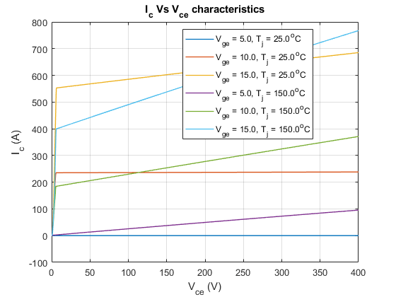
IV Characteristics Simulation Results
IV Characteristics at Full Range
This plot shows IGBT IV curve for  from 0 to
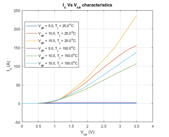
IV Characteristics Near Vce(sat)
This plot shows IV curve near IGBT on-state  voltage from 0 to
Simulated Switching Loss Characteristics for Single Turn-On and Turn-Off
The IGBT switching loss values change according to the definition of the switching region and reverse recovery of the freewheeling diode. In this example, some of the diode reverse recovery is part of the turn-on switching region and any power loss (Vce*Ice) greater than lossFactor*max(Vce*Ice) is a switching loss. This example uses lossFactor of 0.02 (2% of max switching power). During switching, any power loss (Vce*Ice) greater than lossFactor*max(Vce*Ice) is considered as a switching loss.
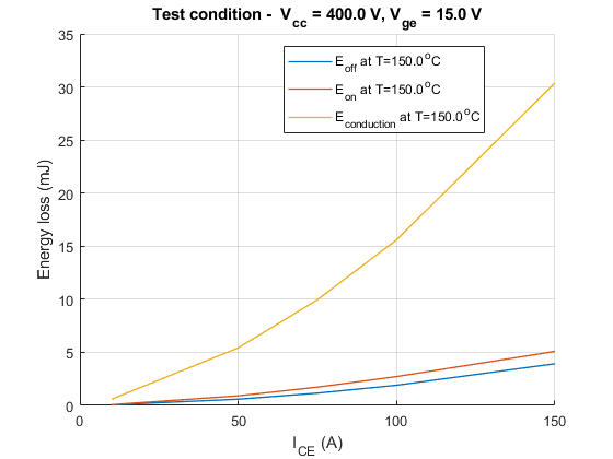
Simulated Loss for Different Ice
This plot shows the simulated loss for different Ice.
Simulated Loss for Different Vce
This plot shows the simulated loss for different Vce.

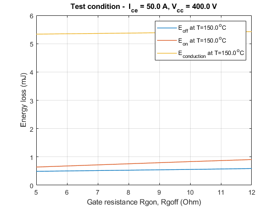
Simulated Loss for Different Rg
This plot shows the simulated loss for different Rg.
Simulated Switching Loss Characteristics for Sinusoidal Load Current and Modulation Signal
Simulated Output for Sinusoidal Load Current
This plot shows the simulated output for the sinusoidal load current when  .
.

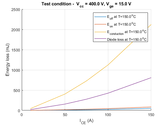
Simulated Loss for Different Collector Current
This plot shows the simulated loss for different Ice when  .
.
Simulated Loss for Different PWM Frequency
This plot shows the simulated loss for different PWM frequencies.

IGBT Junction and Case Temperature Simulation Result
Simulated IGBT case and junction temperature

See Also
IGBT (Ideal, Switching) | N-Channel IGBT | Diode | Heatsink | Gate Driver | Optocoupler | Nonlinear Transformer