F2837xD/F2838x/F2838x-M4 IPC Receive
Receive data from either core while using separate model for each core
Libraries:
C2000 Microcontroller Blockset /
F2837xD
C2000 Microcontroller Blockset /
F2838x /
C28x
C2000 Microcontroller Blockset /
F2838x /
M4
C2000 Microcontroller Blockset /
F28p65x
Description
The IPC Receive block receives and outputs data sent from one Core to the other.
Note
Use IPC Receive and IPC Transmit blocks to receive or sent data to either core for multi-core processors. Use these blocks for flat model approach where you are using separate models for each core.
If you are using multiprocessor modeling approach with single model triggering multiple cores using Task Manager, use the Interprocess Data Read and Interprocess Data Write blocks to send and receive data between cores.
Core1 transmits data to its allocated memory (Core1-to-Core2 Message RAM) and receives data from the allocated memory of Core2 (Core2-to-Core1 Message RAM). Similarly Core2 transmits data to its allocated memory (Core2-to-Core1 Message RAM) and receives data from allocated memory of Core1 (Core1-to-Core2 Message RAM). For F2838xD, Core1/Core2 can be CPU1,CPU2 or ARM Cortex-M4 (CM) and for F2837xD, Core1/Core2 can be CPU1 or CPU2.
If Core1 and Core2 are both C28x core, then the data and channel structure between two cores are allocated in Message RAM and the data array is allocated in Global Shared RAM. In C28x core, by default all the channel structures are created in Message RAM.
However, if one of the core is ARM Cortex M4 (applicable only for F2838x), then the data array is allocated only using Message RAM as global shared RAM is not available between cores. In order to accommodate more data, only required channel structures are created in Message RAM. Hence if the channel number used for transmit block in one core does not match with the receive block in other core the data transmission will not occur.

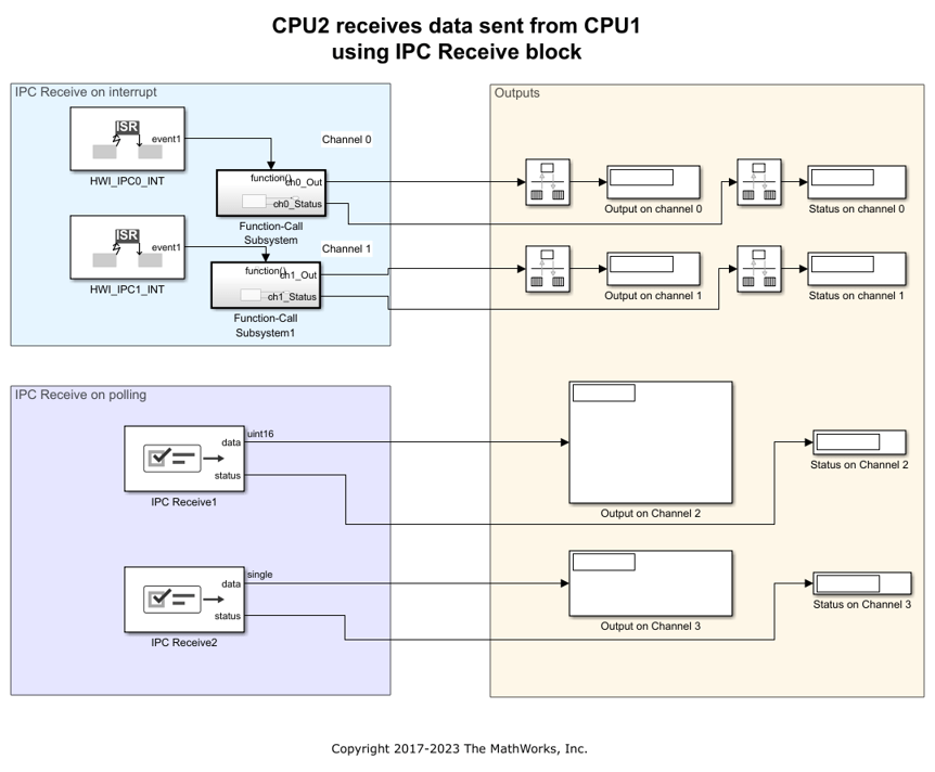
A hardware interrupt block can be used along with the IPC Receive block for receiving data based on hardware interrupts.
C28x processor - Channels 0, 1, 2, and 3 are configured for hardware interrupts IPC0, IPC1, IPC2, and IPC3 respectively.
F2838x-M4 processor - Channels 0, 1, 2, 3, 4, 5, 6 and 7 are configured for hardware interrupts IPC0, IPC1, IPC2, IPC3, IPC4, IPC5, IPC6 and IPC7 respectively.
These hardware interrupts can be set in the hardware interrupt block using these
parameters: CPU interrupt number
1 and PIE interrupt numbers
13, 14, 15, and
16 respectively.
Memory Allocation for IPC Flat Models
The Channel assignment, Memory usage in CM message RAM, and Memory usage in C28x message RAM provides detailed description on how the memory is allocated in IPC blocks for flat models.
Channel assignment - The channel assignment in the C28x-CM IPC (Inter-Processor Communication) is a crucial aspect for seamless communication between CPU1, CPU2, and the Communication Manager (CM). Internally, channel arrays are maintained for each CPU, facilitating data exchange with the CM. This process involves sorting the arrays to allocate channels based on a predetermined order, maximizing the utilization of message RAM for efficient communication.
IPC block sorts the array and allocates the channels based on the sorted order which may result in channel selection on block not matching with channel selection on generated code. This logic helps us to maximize the full use of message RAM to communicate with CPUx and CM.
For example, based on the channel selection on the model:
CM-CPU1 channel selection - if CM-CPU1 array is sorted like
[0_Rx, 0_Tx, 1_Tx, 2_Rx, 4_Rx]then the corresponding entries in generated code would be[0_Rx, 0_Tx, 1_Tx, 2_Rx, 3_Rx].CM-CPU2 channel selection - if CM-CPU2 array is sorted like looks like
[0_Rx, 0_Tx, 2_Rx, 3_Tx, 5_Tx, 6_Tx]then the corresponding entries in generated code would be[0_Rx, 0_Tx, 1_Rx, 2_Tx, 3_Tx, 4_Tx].
Memory usage in CM message RAM - CM message RAM creates the following variables with IPC structure and buffers when IPC Transmit or Receive block is configured in the model. For example, when Buffer size = 2:
MW_IPCCMtoCPUxBuffers - number of elements = (number of channels * Buffer size) - size = 8 bytes to store datatype, data length and data as structure
MW_Cpu1PutWriteIndexes - number of elements = number of channels - size = 2 bytes
MW_Cpu1GetReadIndexes - number of elements = number of channels - size = 2 bytes
MW_CPU1WRITEFLAGBUFF1 - number of elements = number of channels - size = 2 bytes
MW_CPU1WRITEFLAGBUFF2 - number of elements = number of channels - size = 2 bytes
MW_CPU1READFLAGBUFF1 - number of elements = number of channels - size = 2 bytes
MW_CPU1READFLAGBUFF2 - number of elements = number of channels - size = 2 bytes
Buffer allocation based on the channel selection and data length
mwCpu1Channel<channelNumber>Buff1
mwCpu1Channel<channelNumber>Buff2 - number of elements = length of data (datalength) - size 4 bytes
Memory usage in C28x message RAM - C28x message RAM creates the following variables with IPC structure and buffers when IPC Transmit or Receive block is configured in the model. For example, when Buffer size = 2:
MW_IPCCPUtoCMBuffers - number of elements = (number of channels * Buffer size) - size = 8 bytes to store datatype, data length and data as structure.
MW_CmPutWriteIndexes - number of elements = number of channels - size = 2 bytes
MW_CmGetReadIndexes - number of elements = number of channels - size = 2 bytes
MW_CMWRITEFLAGBUFF1 - number of elements = number of channels - size = 2 bytes
MW_CMWRITEFLAGBUFF2 - number of elements = number of channels - size = 2 bytes
MW_CMREADFLAGBUFF1 - number of elements = number of channels - size = 2 bytes
MW_CMREADFLAGBUFF2 - number of elements = number of channels - size = 2 bytes
Buffer allocation based on the channel selection and data length.
mwCmChannel<channelNumber>Buff1
mwCmChannel<channelNumber>Buff2 - number of elements = length of data (datalength) - size 4 bytes
Examples
Ports
Output
Parameters
Version History
Introduced in R2018a

