基于 MCU 的 C2000 DC-DC 降压转换器
本示例展示了如何开发 DC-DC 降压转换器电源调节器应用程序。电源转换仿真和部署中常见的挑战包括:
对降压转换器电路的模拟电路行为进行建模
对 MCU 上 PWM 输出和 ADC 采样的时序特性进行建模
在高 CPU 负载控制器中捕获信号
控制器验证所需的时间,通常在硬件上执行。
本示例使用 C2000™ Microcontroller Blockset 和 Simscape™ 来解决这些挑战。本例中使用的数字控制类型为电压模式控制器 (VMC),已在 TI Delfino F28379D LaunchPad 和 TI BOOSTXL-BUCKCONV 套件上验证。
所需硬件
硬件连接
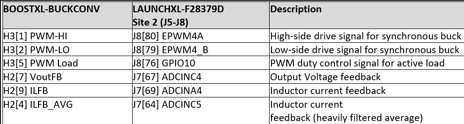
按照下表中的详细说明,将数字电源降压转换器 BoosterPack (BOOSTXL-BUCKCONV) 连接到 Texas Instruments Delfino F28379D LaunchPad。
该模型展示了完整的转换器系统,本示例中的各个部分将探讨各个挑战。打开 soc_dcdc_buck 模型。
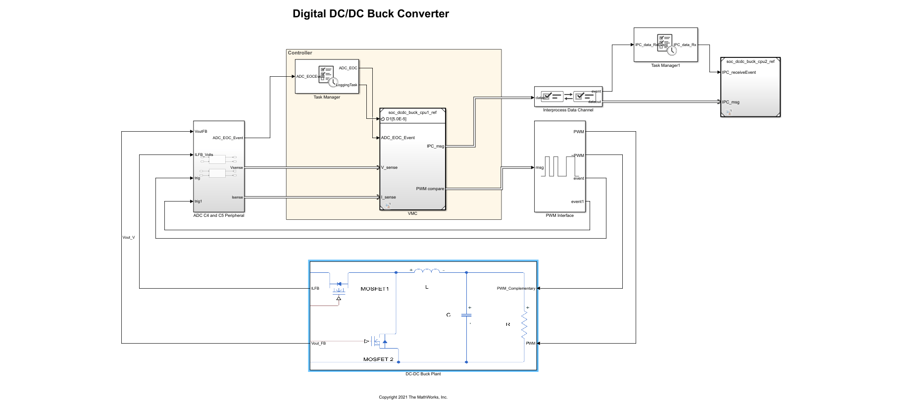
直流-直流降压转换器套件模型
DC-DC Buck Plant 子系统是 DC-DC 降压转换器模拟电路的 Simscape 参考模型。
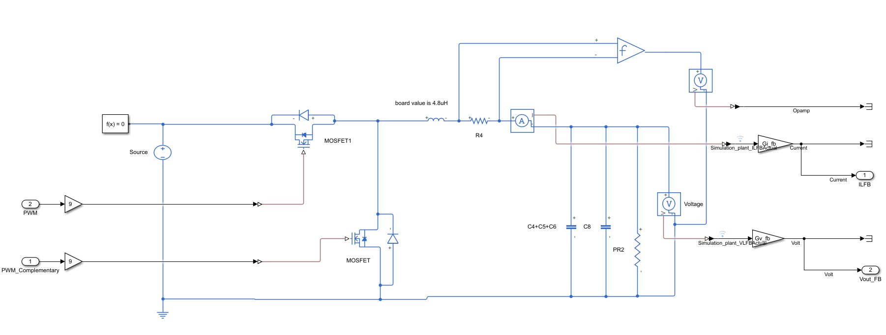
模型中的 Simscape™ 模块是根据数据表中提供的原始设备制造商 (OEM) 规格进行选择和配置的。为了在不影响行为的前提下提高仿真计算效率,该模型相对于原始设备制造商 (OEM) 的规范进行了以下简化:
如果需要,可以使用数字示波器将 Simscape 模型的开环响应与物理硬件进行比较和验证,并使用 Data Acquisition Toolbox 捕获结果。
MCU 上的电压模式控制
在 MCU 上,ADC Interface 对工厂的输出进行采样,在转换的每个末端生成一个事件。Task Manager 在收到每个 ADC 转换结束事件时执行一个名为 ADC 的事件驱动任务。ADC 中断任务包含反馈控制算法,该算法异步执行以响应每个 ADC 转换事件。控制算法通过 ADC 读取接收反馈,并为 PWM Write 模块生成占空比值。PWM Interface 模块仿真 PWM 行为,包括触发事件以开始下一次 ADC 转换。PWM 频率设置为 200 kHz。离散比例积分 (PI) 控制器可最大限度地减少参考电压和输出电压之间的误差。PI 控制器的占空比限制为 PWM 时间周期的 40%。
该系统从 1 伏的初始电压参考值开始,并允许其达到稳态。这样就可以在物理硬件和仿真之间进行公平的控制,以便与已知状态进行比较。然后,在 50 毫秒时触发 2 伏的期望电压阶跃,以检验闭环控制器的阶跃响应。点击播放来仿真模型。打开仿真数据检查器并查看信号。
为了验证仿真结果与硬件的一致性,将模型部署到 Texas Instruments Delfino F28379D LaunchPad 上。在 System on Chip 选项卡上,点击 Configure, Build, & Deploy 以打开 SoC 构建器工具。该图显示了仿真和部署在物理硬件上的模型之间控制器响应的比较。使用数字示波器捕获硬件上的该信号。控制器的高频运行阻止了在同一 CPU 上直接使用外部模式。因此,需要使用数字示波器来进行这些测量。
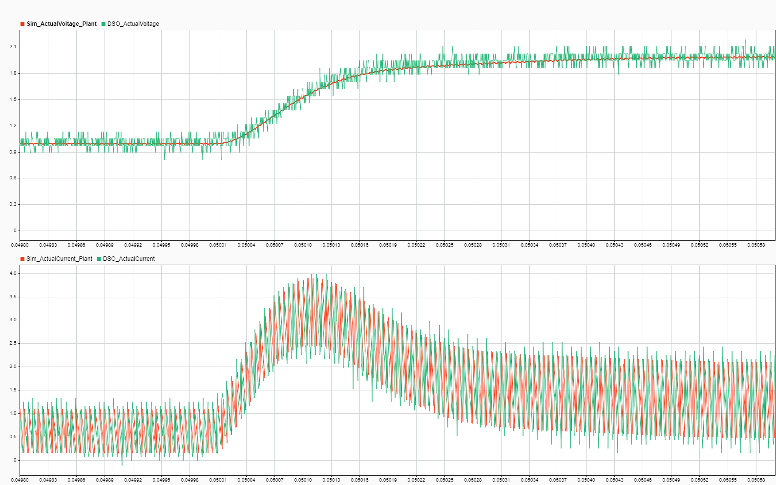
正如预期的那样,电压模式控制器能够正确跟踪所需的电压输出。此外,对于此类系统,已部署模型的测量结果与仿真的吻合度超过 95%。仿真和部署测量之间出现的细微差异可归因于 Simscape 模型中所做的简化。
利用多核处理器在 CPU2 上记录数据
CPU2 配置为运行外部模式的 SoC 构建器工具,以记录和传输 CPU1 上的控制回路产生的高频信号。Interprocess Data Channel 模块连接 CPU1 和 CPU2,在 CPU 之间提供低延迟数据传输。
使用 SoC 构建器工具将模型部署到 TI Delfino F28379D LaunchPad。由 SoC 构建器工具建立的主机-目标通信连接,记录硬件板 CPU2 上运行的可执行文件的信号数据,并将数据发送到 Simulink 中的仿真数据检查器。使用 CPU2 来拥有和管理主机-目标通信和数据记录,可以从 CPU1 上资源密集型、高优先级任务中捕获数据,而不会干扰其行为,并使该任务能够消耗大部分 CPU 资源,同时保持数据记录的质量达到 Simulink。该图显示了部署到 TI Delfino F28379D LaunchPad 的模型在 CPU1 上执行任务 1 时,在 CPU2 上执行任务 2 时记录的数据信号。
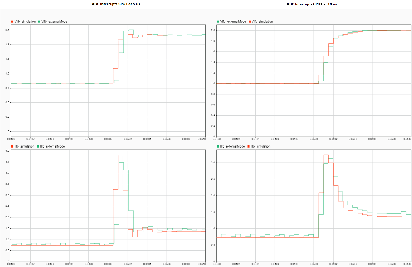
ADC 转换触发的起始点可以配置为在第一个 PWM 或第二个 PWM 事件时生成。这些设置在仿真和代码生成中均可用。观察仿真和代码生成结果,准确率超过 95%。
任何资源密集型 C2000 Blockset 模型都可以使用此设置,在将模型部署到 TI Delfino F28379D LaunchPad 时记录来自硬件的数据。
进一步探索
扩展适用于涉及氮化镓 (GaN) 或碳化硅 (SiC) 的高频开关应用
可变脉宽调制频率和固定占空比
可变相位偏移
通过使用 PWM 输出控制选项,可以实现不同的 PWM 输出方案。
不同的 PWM 事件生成技术