Model SPI Communication
R2026bSPI is a full-duplex serial protocol that uses a shift register for data transfer. Modeling SPI communication correctly in Simulink® ensures that the generated code communicates reliably with peripheral devices when you deploy to TI’s C2000™ hardware.
For every bit the controller shifts out on MOSI, the peripheral simultaneously shifts one
bit back on MISO. This bidirectional behavior applies to both read and write operations and
determines how you structure your SPI model. The c28x_spi_eeprom_interrupt
model, which communicates with a CAT25256 EEPROM device, illustrates these patterns throughout
this topic.
Before you configure SPI communication, select a C2000 hardware board in your model configuration parameters and connect an SPI peripheral device to the appropriate pins on the board.
Depending on your application requirements, you can model SPI communication using one of two approaches:
Blocking mode — The processor waits until the transfer completes. Use this mode for straightforward communication with a single peripheral.
Interrupt mode — The processor continues executing other tasks during the transfer. Use this mode for time-critical applications with multiple peripherals.
SPI Data Transfer: Shift Register Mechanism
The SPI shift register exchanges one bit in each direction for every clock cycle. When the controller transmits data, the peripheral simultaneously shifts data back. This exchange means every SPI transaction produces both transmitted and received data, regardless of whether the application needs both directions.
This bidirectional mechanism has two practical consequences for your model:
Write operations produce junk receive data. When the controller writes to the peripheral (for example, sending an EEPROM write command), the peripheral shifts back whatever its shift register holds. Discard this data in your model.
Read operations require dummy transmit data. When the controller reads from the peripheral (for example, reading an EEPROM memory location), the controller must transmit dummy bytes to generate the clock cycles that shift data out of the peripheral.
Simultaneous Data Transfer on SPI Bus
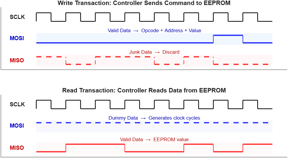
In the EEPROM example, the Write Data subsystem demonstrates a write operation where received junk data is discarded, and the Read Data subsystem demonstrates a read operation where the controller transmits dummy bytes to clock out the stored EEPROM value.
Blocking Mode: Transfer Data with Single Block
The simplest way to model SPI communication is with the C28x/C29x SPI Controller Transfer block. This block handles both transmit and receive operations internally, eliminating the need to pair separate blocks or configure interrupts.
In blocking mode, the processor waits until the block transfers all data before continuing execution. This approach works well when your application communicates with a single peripheral and does not have strict timing constraints on other tasks.
When using the SPI Controller Transfer block:
Do not use C28x/C29x SPI Transmit or C28x/C29x SPI Receive blocks in the same model for the same SPI module.
Do not configure SPI interrupts, as the block manages the complete transfer sequence internally.
The SPI Controller Transfer block manages the chip select (CS) pin automatically — it sets CS low before data transfer and sets CS high after the entire transfer completes. For reliable multi-byte transfers, set the CS pin mode to Explicit GPIO calls as described in Configure Chip Select Pin.
Blocking mode wastes processor time when your application uses multiple SPI peripherals. Because the processor is idle during each transfer, blocking mode accumulates dead time across all modules. Interrupt mode eliminates this idle time.
Interrupt Mode: Transfer Data with Separate Blocks and ISR
For applications where blocking the processor is unacceptable — such as control loops with tight timing requirements or systems with multiple SPI peripherals — use interrupt mode. In this mode, the C28x/C29x SPI Transmit block starts the transfer, and an interrupt notifies the processor when data arrives. The processor executes other tasks during the transfer instead of waiting.
Pair SPI Transmit and Receive Blocks
Because SPI uses a shift register, you must use the SPI Transmit block and the C28x/C29x SPI Receive block together on the controller side. When the SPI Transmit block shifts out data, the SPI Receive block reads the data simultaneously shifted in from the peripheral device.
To model a controller-side transmit operation:
Add an SPI Transmit block and an SPI Receive block to your model.
Connect the transmit data to the SPI Transmit block input.
Complete each transmit-receive sequence before starting the next transfer.
Discard the data from the SPI Receive block output during write operations.
Paired SPI Transmit and Receive Blocks in Write Enable Subsystem

In the EEPROM example, the Write Enable subsystem demonstrates this pattern — paired SPI Transmit and SPI Receive blocks where the received junk data is discarded.
Configure Interrupts for Non-Blocking Transfer
To prevent data loss during SPI communication, configure interrupts so the processor does not need to poll for transfer completion.
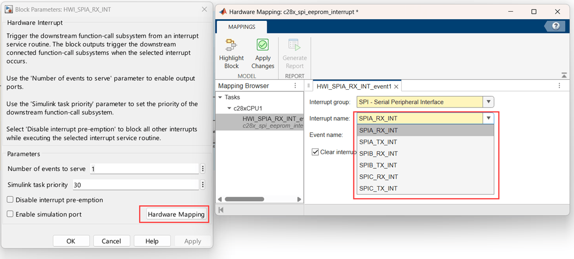
On the Hardware tab, click Hardware Mapping. In the Hardware Mapping tool, enable the transmit or receive interrupt for the corresponding SPI module. Each SPI module supports separate interrupts for transmit and receive operations.
SPI Interrupt Options in Hardware Mapping Tool
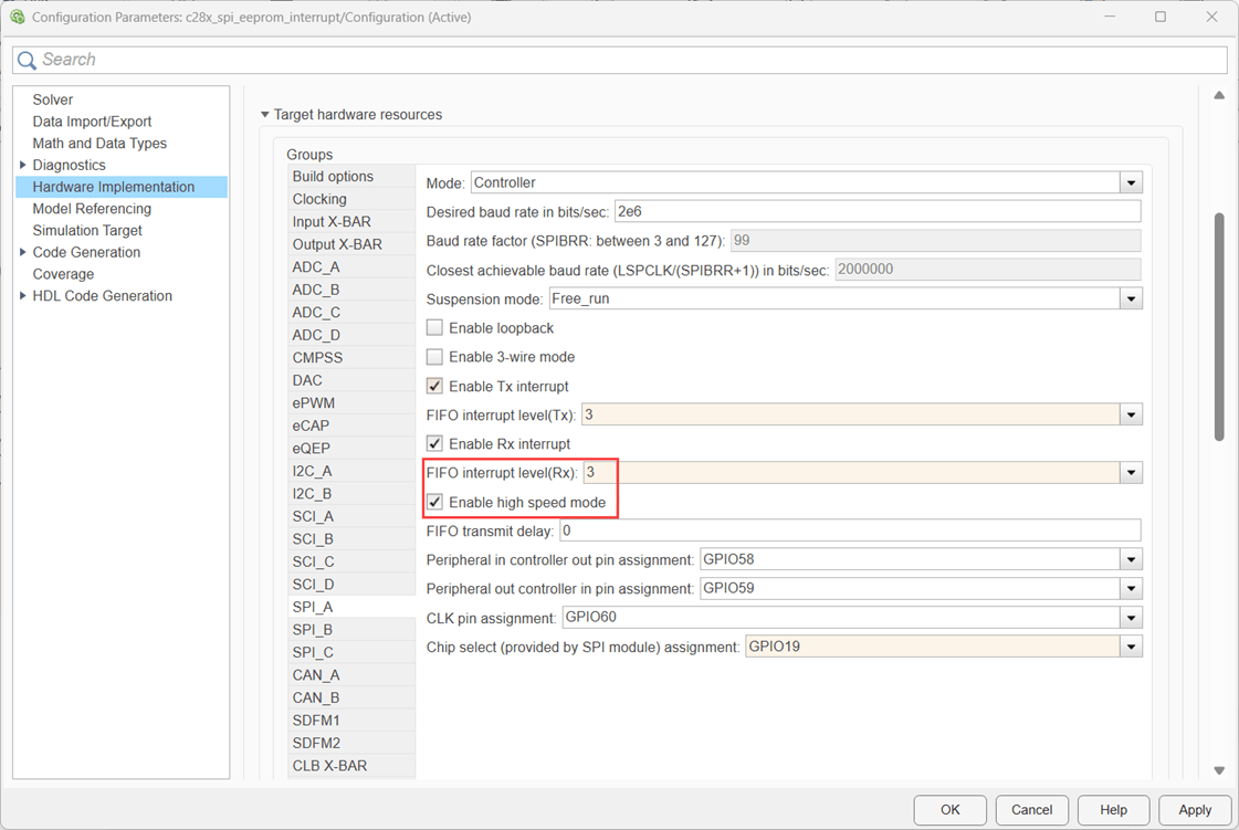
In the Configuration Parameters dialog box, in the Target hardware resources section for the SPI module, set the FIFO interrupt level (Rx) parameter to specify the number of received bytes that trigger the interrupt. Set the value to match the number of data bytes in each SPI transaction. For example, if each transaction transfers 4 bytes, set the FIFO interrupt level to 4.
FIFO Interrupt Level in Target Hardware Resources
In the interrupt service routine (ISR), use the SPI Receive block to read and process (or discard) the received data.
For a complete implementation of interrupt-based SPI communication, see the
c28x_spi_eeprom_interrupt model in the Using SPI to Read and Write Data to SPI EEPROM example.
Manage Chip Select Pin in Interrupt Mode
Because the SPI Transmit and SPI Receive blocks operate independently, they each control one transition of the CS pin:
- SPI Transmit
Sets CS low before data transfer.
- SPI Receive
Sets CS high after data reception.
You must use both blocks together to complete the CS pin assertion cycle. The SPI blocks manage the CS pin — you do not need to configure its state manually using Digital Output blocks.
Compare Blocking and Interrupt Modes
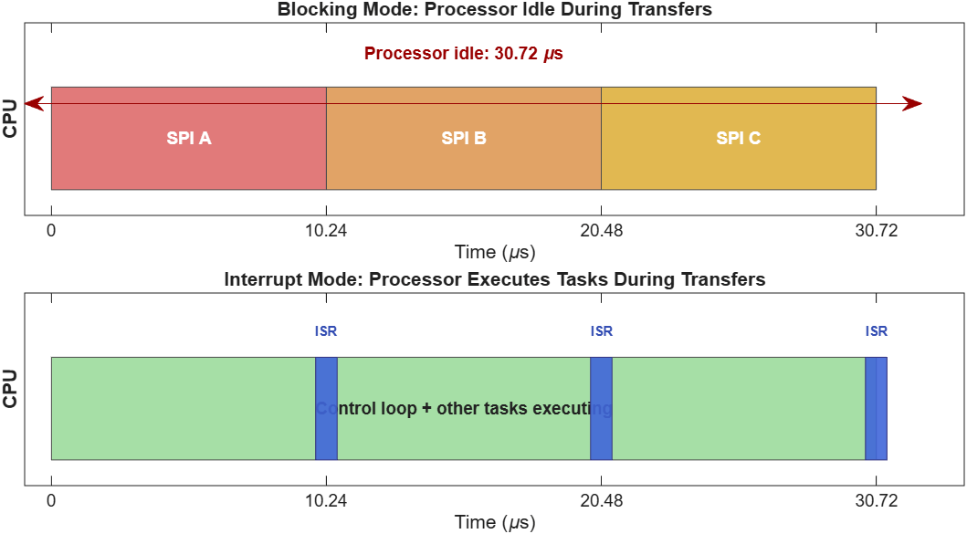
The choice between blocking and interrupt modes primarily affects processor utilization. For example, with three SPI modules (A, B, C), each transmitting 4 uint16 values at a bit rate of 6.25 Mbps:
Blocking mode (SPI Controller Transfer):
Time per bit = 1/6.25 MHz = 0.16 µs
Transfer time per module = 4 × 16 bits × 0.16 µs = 10.24 µs
Total processor time blocked = 3 × 10.24 µs = 30.72 µs
In blocking mode, the processor is idle during the entire 30.72 µs transfer duration.
Interrupt mode (SPI Transmit and Receive):
The SPI Transmit block starts the transfer for each module.
The processor continues executing other tasks during the transfer.
When the receive interrupt triggers, the ISR reads and discards junk data.
In interrupt mode, the processor is free to execute other tasks during the transfer, significantly improving utilization in applications with multiple SPI peripherals or time-critical control loops.
Processor Utilization in Blocking Mode vs. Interrupt Mode
Configure Chip Select Pin
Regardless of which transfer mode you use, set the chip select (CS) pin mode to Explicit GPIO calls on both the controller and peripheral sides. This setting gives the generated code full control over the CS pin state, independent of the SPI peripheral hardware behavior.
The CS pin is active low — it is asserted (low) when the peripheral is selected and deasserted (high) when the peripheral is released. The two CS pin modes behave differently during multi-byte transfers:
Provided by the SPI peripheral — The hardware controls the CS pin based on the FIFO state. If the FIFO empties between bytes, the CS pin de-asserts (goes high) prematurely, even if the transfer sequence has not completed.
Explicit GPIO calls — The generated code keeps the CS pin asserted (low) until all data bytes in the transfer sequence complete.
On the peripheral side, the controller drives the CS pin. The SPI Receive block on the peripheral has no effect on the CS pin state, but you should still set the mode to Explicit GPIO calls for consistent configuration.
Model SPI Peripheral Communication
If your C2000 board operates as an SPI peripheral (receiving commands from an external controller), the configuration is simpler than the controller side.
On the peripheral side, use only the SPI Receive block. You do not need a separate SPI Transmit block because the SPI Transmit block shifts out whatever data the shift register currently holds, which is not the intended behavior for a peripheral receiver. Configure the SPI Receive block with the same SPI mode (clock polarity and phase) and bit rate as the controller side to ensure proper communication.
SPI EEPROM Example: Write and Read Sequences
The c28x_spi_eeprom_interrupt model demonstrates the SPI modeling
patterns described in this topic. The model communicates with a CAT25256 EEPROM device using
interrupt-mode SPI, with paired Transmit and Receive blocks and a state machine that sequences
the operations.
SPI EEPROM Interrupt Example Model Architecture
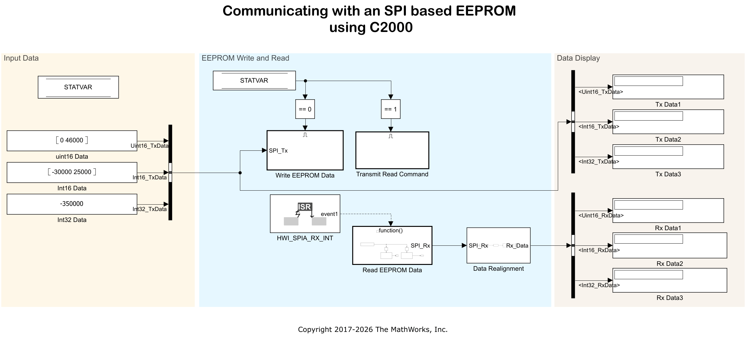
The EEPROM uses an instruction set where each transaction includes an opcode, address, and data payload.
Write Sequence
To write to a memory location, the controller transmits a frame in the format [Opcode, Address, Value], where the opcode for write is 2. Because the shift register always transfers data in both directions, the peripheral shifts junk data back to the controller during this operation. The model discards this data.
In the example model:
The Write Data subsystem (inside Write EEPROM Data) transmits the write command using paired SPI Transmit and SPI Receive blocks.
The Read Dummy Data subsystem (inside Read EEPROM Data) reads and discards the junk data received during the write.
Write Data Subsystem in EEPROM Example
![Write Data subsystem showing three inputs — Write Command (opcode 2), Write Address [0 32], and Data — multiplexed through a Mux block into the SPI Transmit block. The SPI Transmit block is configured with Chip select: GPIO1. A Constant block with value 2 connects to the STATVAR data store to advance the operation state.](spi_eeprom_write_subsystems.png)
Read Sequence
To read a memory location, the controller transmits a frame in the format [Opcode, Address, Junk], where the opcode for read is 3. The junk byte provides the clock cycles needed for the peripheral to shift out the stored value.
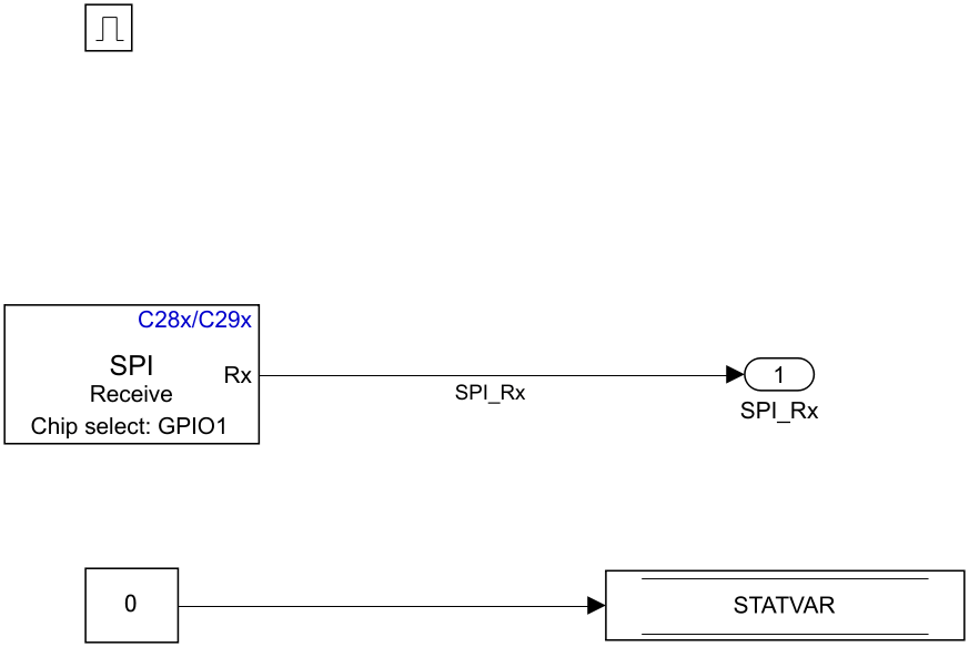
In the example model, the Read Data subsystem (inside Read EEPROM Data) receives the
valid data from the EEPROM. The STATVAR data store controls the sequence
of write and read operations and transitions the model through its operation states.
Read Data Subsystem in EEPROM Example
Troubleshoot SPI Communication
If SPI communication does not work as expected after deployment, verify the following configurations:
- Bit rate mismatch
Verify that the controller bit rate matches the specifications in the peripheral device datasheet. A mismatch causes data corruption or communication failure.
- Incorrect SPI mode
Configure the SPI mode (clock polarity and clock phase) to match the mode supported by the peripheral device. Refer to the peripheral datasheet for the required CPOL and CPHA settings.
- Mixed block usage with Controller Transfer
When using the SPI Controller Transfer block, do not use SPI Transmit, SPI Receive, or interrupts for the same SPI module. The Controller Transfer block operates in blocking mode and manages the complete transfer sequence internally.
- Missing SPI Receive block
When using the SPI Transmit block, always include a corresponding SPI Receive block. The shift register mechanism requires both blocks to complete a transfer.
- Unhandled junk data
During write operations, discard the junk data received from the peripheral. During read operations, transmit dummy data to generate the clock cycles needed to receive valid data from the peripheral.
- Incomplete transfer before next byte
Verify that each transmit-receive transaction completes before starting the next byte transfer. Overlapping transfers cause data corruption.
- Unstable chip select signal
Set the CS pin mode to Explicit GPIO calls to prevent premature CS assertion between bytes during multi-byte transfers.
- Incorrect interrupt configuration
Verify that you configured the FIFO level and interrupt event settings correctly for the corresponding SPI module. The FIFO interrupt level must match the expected number of bytes per transaction.
- Incorrect command sequence
Follow the read and write sequence specified in the peripheral device datasheet. If the device requires an opcode before data, transmit the opcode first.
After you configure your SPI model, deploy it to your C2000 hardware to verify communication with the peripheral device. If you encounter communication issues, use the troubleshooting checklist in this section to diagnose common configuration errors.
See Also
C28x/C29x SPI Controller Transfer | C28x/C29x SPI Receive | C28x/C29x SPI Transmit

