Verify OFDM Transmit and Receive using FPGA Data Capture
This example shows how to verify a wireless HDL IP that you generate in OFDM Transmit and Receive Using Analog Devices AD9361/AD9364 (SoC Blockset). The example also shows how to monitor and analyze the internal signals of an IP core using FPGA data capture on real hardware.
You use the FPGA Data Capture tool to capture the hardware signals over JTAG for debugging analysis. FPGA data capture offers many capabilities to capture signals of interest using appropriate trigger and capture conditions. You validate the behavior of the whdlOFDMRx Model subsystem in the zynqRadioHWSWOFDMAD9361AD9364SL model by performing these steps.
Use capture control to capture valid data constellation points.
Use trigger conditions and multiple windows to capture header constellation points for frames with a failed CRC.
Use trigger conditions and the trigger position to capture synchronizing sequence (SS) correlation data for the peak search and validate the timing offset.
Requirements
To run this example, you need an AMD® Zynq® ZC706 evaluation kit and FMCOMMS2/3/4 radio transmitter hardware.
Hardware Setup
Follow the steps in Set Up AMD FPGA and SoC Devices (SoC Blockset) to configure the host computer and ZC706 board with FMCOMMS2/3/4 radio hardware.
Use the JTAG cable to connect the board to the host computer.
Simulink Model Setup
Open zynqRadioHWSWOFDMAD9361AD9364SL.slx model.
Mark the signals that you want to analyze through data capture as test points. To mark a signal as a test point, right-click the signal and then click Properties. On the Signal Properties dialog box, on the Logging and accessibility tab, select the Test point checkbox, as this figure shows.
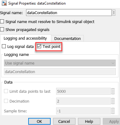
Alternatively, use the hOFDMTxRxAddTestPoints helper function to mark the required test points and save the model as zynqRadioHWSWOFDMAD9361AD9364SLVerify. The function is attached to the example as a supporting file.
hOFDMTxRxAddTestPoints
This figure shows the test points marked in the whdlOFDMRx Model subsystem for capturing the header and data constellation points.

This figure shows the test points marked in the Sync Signal Search subsystem for capturing the SS correlation and timing offset signals.

Generate HDL IP Core with Data Capture and Load Bitstream
Start the targeting workflow by right-clicking the
OFDM HDLsubsystem and selecting HDL Code > HDL Workflow Advisor.In step 1.1, set Target workflow to
IP Core Generationand Target platform toZC706 and FMCOMMS2/3/4.In step 1.2, set Reference design to
Receive and Transmit path. For this example, you can use the default values of the reference design parameters.In step 1.3, select Enable HDL DUT output port generation for test points to update the interface table with all the test points. Then, in the Target platform interface table, map the test point signals to
FPGA Data Capture. For information about mapping IO ports, see OFDM Transmit and Receive Using Analog Devices AD9361/AD9364 (SoC Blockset).
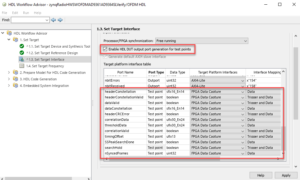
Run step 1.4 to step 3.1 by following the Generate IP Core section of the OFDM Transmit and Receive Using Analog Devices AD9361/AD9364 (SoC Blockset) example.
In step 3.2, set FPGA data capture buffer size to
32768and FPGA data capture maximum sequence depth to2. Select Include capture condition logic in FPGA Data Capture to insert the capture control logic into the generated FPGA data capture component, as this figure shows.
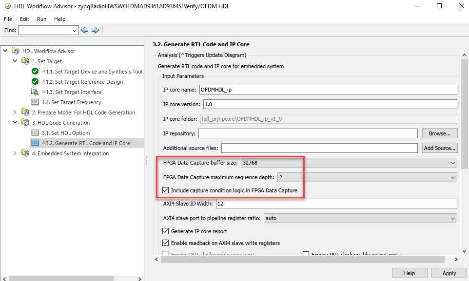
Run step 4.1 and follow the steps in the Generate Software Interface Model and Block Library section of the OFDM Transmit and Receive Using Analog Devices AD9361/AD9364 (SoC Blockset) example to generate a software interface model.
To generate and download the bitstream onto the board, follow the Generate and Load Bitstream section of the OFDM Transmit and Receive Using Analog Devices AD9361/AD9364 (SoC Blockset) example.
Alternatively, run the hOFDMTxRxRunHDLWATasks helper function to run the tasks from step 1.1 to step 4.3. The function is attached to the example as a supporting file.
hOFDMTxRxRunHDLWATasks
Capture and Analyze Data from IP Core
Capture the test points of the generated IP core and map them to FPGA data capture. To run the software interface model while the FPGA data capture waits for a trigger, launch the FPGA Data Capture tool in nonblocking mode.
cd(fullfile('hdl_prj','hdlsrc', ...
   'zynqRadioHWSWOFDMAD9361AD9364SLVerify','fpga_data_capture'));
fdc = FPGADataCapture;
fdc.CaptureMode = 'nonBlocking';
fdc.launchApp;
Open the OFDM software interface model. Run the model in Monitor & Tune mode to control the configuration from the Simulink model.
open_system('zynqRadioHWSWOFDMAD9361AD9364SL_interface');
Capture Data Constellation Points
Use the frequency-domain, channel-equalized, and common-phase-error (CPE) corrected data subcarriers from the Channel and CPE Estimation and Correction subsystem to plot the data constellation diagram. To capture only valid data constellation points, select Enable capture condition logic on the Capture Condition tab of the FPGA Data Capture tool and add tp_dataValid_1 as a signal with value High, as this figure shows. Click Capture Data.

After data capture is complete, plot the constellation diagram using the data that the board captures.
When enableInternaLoopback in the software interface model is false, the radio hardware transmits and receives the OFDM signals through the Tx and Rx antennas, respectively. The channel impairments modify the signal as it travels over the air in real time. In this scenario, use the constellation plot to analyze the received signal quality. You can also modify modType in the software interface model and verify the data constellation diagram appears as you expect.
hOFDMTxRxPlotDataConstellationFDC

Capture Header Constellation Points for Failed CRC
When the signal-to-noise ratio (SNR) of the channel is low, the valid header data after channel equalization and CPE correction often has CRC failures. You can emulate these conditions using the software interface model.
In the software interface model, set enableInternalLoopback to true and snrdB to 3. Use these trigger settings to capture the I/Q data of two header frames when the CRC fails.
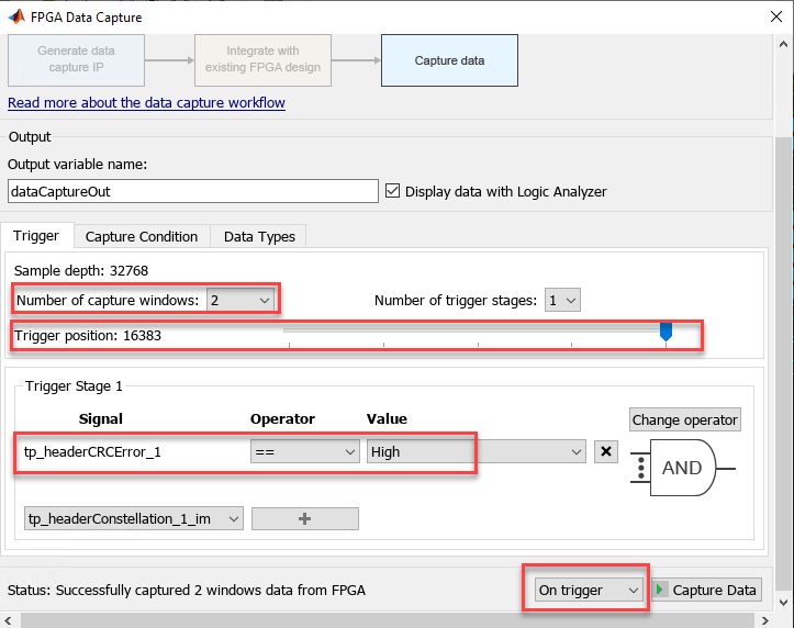
Click Capture Data. The Logic Analyzer app plots the captured data as multiple signal waveforms. The signal tp_nSyncedFrames in the captured data indicates the number of the frame with a failed CRC.

Validate Functionality of Sync Signal Search Subsystem
The Sync Signal Search subsystem implements the SS correlation. The subsystem performs SS detection by continuously cross-correlating the received signal with the SS signal in the time domain. In addition, the subsystem computes the energy of the signal in the span of the correlator at each time step and then scales the value to generate a threshold value. The Max Peak Searcher subsystem searches for the maximum correlation peak in each OFDM frame duration. In the Sync Signal Search subsystem, the SearchHold signal disables maximum peak search until it estimates the carrier frequency offset. The SSPeakSearchDone signal goes high after the completion of peak search in each OFDM frame duration. For an FFT Length of 128, the frame duration is 5760 samples. The position of the maximum peak from the start of the frame duration gives the timing offset. You can capture valid samples of correlation in each OFDM frame duration to visualize the correlation data and record the timing offset.
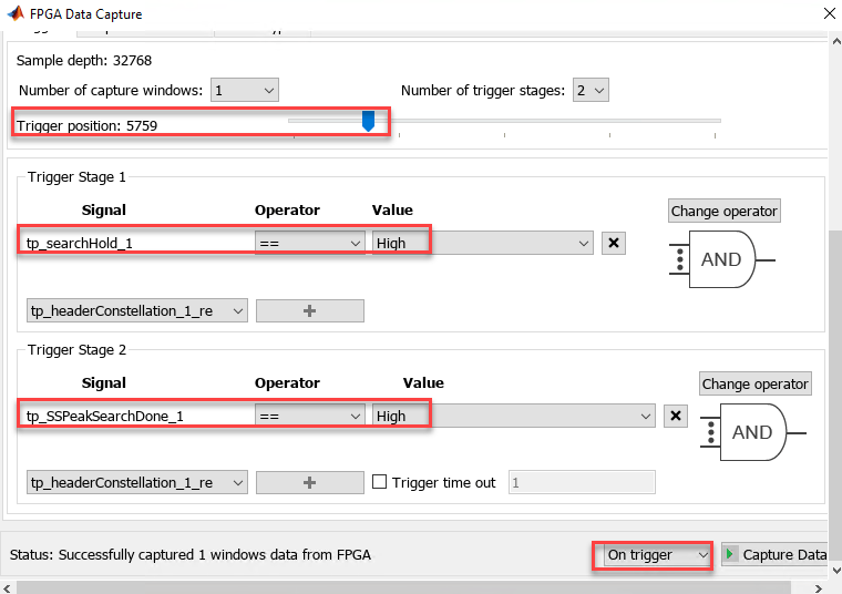
On the Trigger tab, add tp_searchHold_1 as a signal with the value High in Trigger Stage 1. To capture correlation data for each frame duration, add tp_SSPeakSearchDone_1 as a signal with the value High in Trigger Stage 2 and set Trigger position to 5759. These settings ensure that the tool captures 5760 valid correlation samples before the signals satisfy these triggers. Samples 5761 to 11520 correspond to correlation of the next OFDM frame duration, and so on.
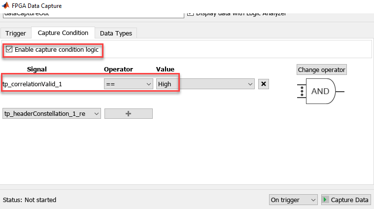
Select Enable capture condition logic on the Capture Condition tab to capture valid correlation data in each frame duration. Add the tp_correlationValid_1 as a signal with the value High, as this figure shows.
Click Capture Data. The Logic Analyzer displays the captured data as multiple signal waveforms.

Run the hOFDMTxRxPlotSSCorrelation helper function to visualize the peak by plotting the captured correlation and threshold values. The index of the peak in each frame relative to start of the frame duration gives the timing offset.
hOFDMTxRxPlotSSCorrelation

Conclusion
This example shows how to map the internal signals of an IP core to FPGA data capture and then visualize the signals after you deploy the design to an FPGA. You use the trigger and capture control configuration of the FPGA Data Capture tool for capturing the signals of interest. You can use this approach to analyze and debug your own HDL IP core.