gerberWrite
R2026bGenerate Gerber files
Syntax
Description
gerberWrite( creates a
Gerber file from PCB specification files, such as designobject)PCBWriter
object or pcbStack object.
Note
To create associated files, run any of the analysis functions such as
show, impedance, pattern etc. on the
antenna before running the gerberWrite
function.
gerberWrite(
creates Gerber file using specified RF connector.designobject,rfconnector)
gerberWrite(
creates a Gerber file using specified PCB writer services.designobject,writer)
gerberWrite(
creates a Gerber file using specified PCB writer and connector services.designobject,writer,rfconnector)
[
creates a Gerber file using specified PCB writer and connector services.a,g] = gerberWrite(designobject,writer,rfconnector)
Note
You can only use output arguments if the
designobject is a pcbStack
object.
Examples
Create a patch antenna with FR4 as a dielectric material using pcbStack object.
p = pcbStack;
d = dielectric("FR4");
d.Thickness = p.BoardThickness;
p.Layers = {p.Layers{1},d,p.Layers{2}};
p.FeedLocations(3:4) = [1 3];
show(p)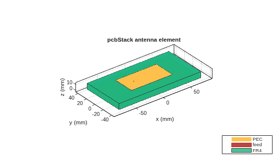
Use a Cinch SMA for feeding the antenna. Use the Mayhew Labs PCB viewer as the 3-D viewer. Change the file name of the Mayhew Writer services to antenna_design_file.
C = PCBConnectors.SMA_Cinch;
W = PCBServices.MayhewWriter;
W.Filename = 'antenna_design_file';
Generate the Gerber-format files.
[A,g] = gerberWrite(p,W,C)
A =
  PCBWriter with properties:

                        Design: [1×1 struct]
                        Writer: [1×1 PCBServices.MayhewWriter]
                     Connector: [1×1 PCBConnectors.SMA_Cinch]
           UseDefaultConnector: 0
    ComponentBoundaryLineWidth: 8
         ComponentNameFontSize: []
            DesignInfoFontSize: []
                          Font: 'Arial'
                     PCBMargin: 5.0000e-04
                    Soldermask: 'both'
                   Solderpaste: 1
               EnableSignature: 1
          EnableConnectorLabel: 1

   See info for details
g =
'/tmp/Bdoc26b_3351752_1297500/tp13aea7fd/antenna-ex85477975/antenna_design_file'
Create a coplanar inverted-F antenna.
fco = invertedFcoplanar(Height=14e-3,GroundPlaneLength=100e-3,...
    GroundPlaneWidth=100e-3);
Use this antenna to create a PCB stack object.
p = pcbStack(fco);
figure
show(p)
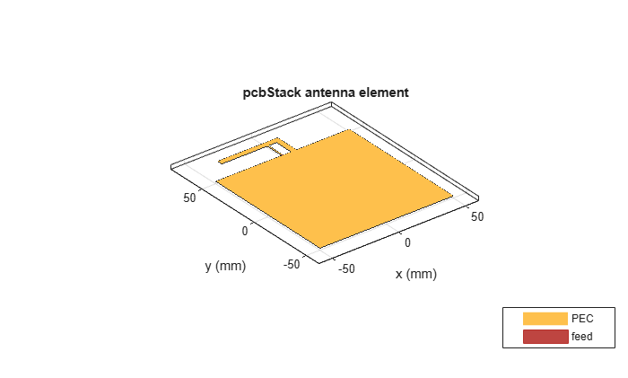
Use the GerbLookWriter to generate the Gerber files for the PCB.
s = PCBServices.GerbLookWriter;
Create an antenna design file using PCBWriter.
PW = PCBWriter(p,s);
Use the gerberWrite method to create Gerber files from the antenna design files.
gerberWrite(PW)
Generated File: 'C:\Users\user\OneDrive - MathWorks\Documents\MATLAB\ExampleManager\user.Bdoc.DocWork0\antenna-ex14839356\untitled.zip'
'(name is available in system cut-buffer)

13 files in PCB stack
   Size Lines File
     1k    64 untitled.gtl (Copper,L1,Top,Signal)
   239b    19 untitled.gts (Soldermask,Top)
   369b    29 untitled.gbs (Soldermask,Bot)
   285b    18 untitled.gbl (Copper,L2,Bot)
   308b    27 untitled.gtp (Paste,Top)
   215b    19 untitled.gbp (Paste,Bot)
   103b     6 untitled.txt (ExcellonPlated,1,2)
   207k 10349 untitled.gto (Legend,Top)
   118k  6204 untitled.gbo (Legend,Bot)
     1k    38 untitled.gpi (PhotoplotterInfo,Info)
     1k    36 untitled.dri (DrillStationInfo,Info)
   239b    17 untitled.ipc (IPCD356A,Info)
              untitled.gml (Profile,NP)
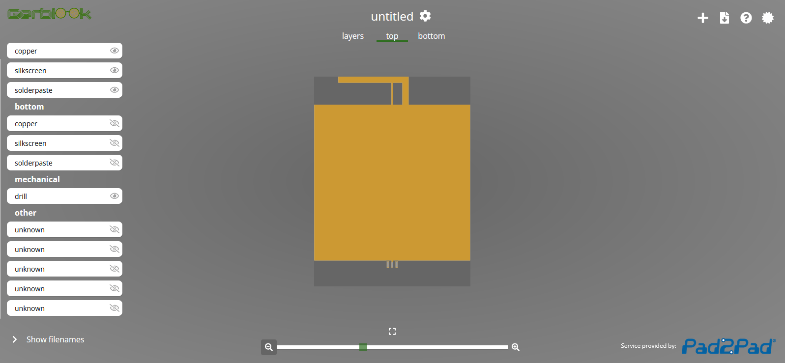
The location of the folder and the GerbLook viewer website opens automatically.
To view the board, drag and drop the files.
Design a patch antenna.
p = design(patchMicrostrip,3.5e9);
p.Width = p.Length;
p.Substrate = dielectric("FR4");
Create a stack representation of the patch antenna.
pb = pcbStack(p);
pb.FeedLocations = [pb.FeedLocations;-.007 0 1 3;0 .007 1 3;0 -.007 1 3];
Pick a connector for the feed locations.
C = SMA_Cinchcustom1;
Pick a manufacturing service.
Wr = PCBServices.GerbLookWriter;
Generate Gerber files.
A = PCBWriter(pb,Wr,C);
gerberWrite(A)
Generated File: 'C:\Users\user\OneDrive - MathWorks\Documents\MATLAB\ExampleManager\user.Bdoc.DocWork1\antenna-ex70748514\untitled.zip'
'(name is available in system cut-buffer)

12 files in PCB stack
   Size Lines File
   126b    10 untitled.gtl (Copper,L1,Top,Signal)
     2k   182 untitled.gbl (Copper,L2,Bot,Signal)
              untitled.gts (Soldermask,Top)
   509b    37 untitled.gbs (Soldermask,Bot)
   132b     8 untitled.txt (ExcellonPlated,1,2)
     1k    98 untitled.gbp (Paste,Bot)
   139k  7250 untitled.gbo (Legend,Bot)
   181k  9132 untitled.gto (Legend,Top)
     2k    54 untitled.gpi (PhotoplotterInfo,Info)
     1k    36 untitled.dri (DrillStationInfo,Info)
     2k    37 untitled.ipc (IPCD356A,Info)
              untitled.gml (Profile,NP)
This is the bottom view of the PCB rendered by the GerbLook online viewer.
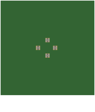
Create a probe-fed microstrip patch antenna with four ports.
p = design(patchMicrostrip(Substrate=dielectric("FR4")),3.5e9);
p.Width = p.Length;
pb = pcbStack(p);
pb.FeedLocations = [pb.FeedLocations;-0.007 0 1 3;0 0.007 1 3;0 -0.007 1 3];
figure
show(pb)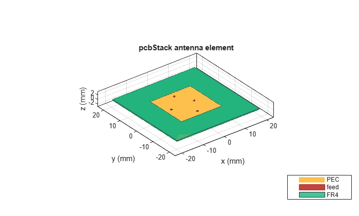
Pick a manufacturing service.
Wr = PCBServices.GerbLookWriter;
Wr.Filename = 'Microstrip antenna-4ports';
Pick a connector for the feed locations.
C = SMA_Cinchcustom1;
Create a Gerber file and generate it.
A = PCBWriter(pb,Wr,C);
A.Soldermask = 'neither';
gerberWrite(A)
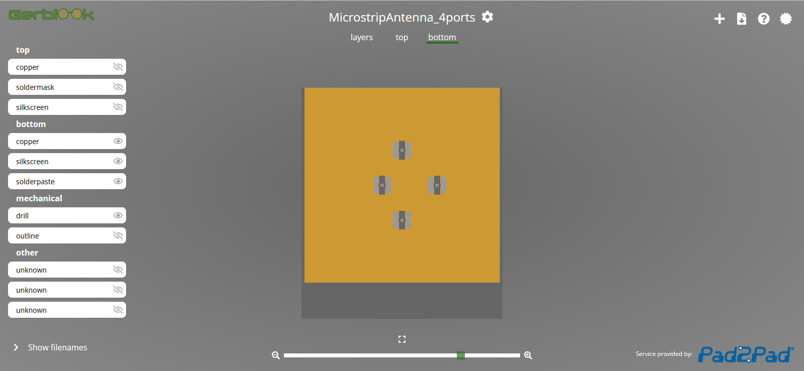
Generated File: 'C:\Users\user\OneDrive - MathWorks\Documents\MATLAB\ExampleManager\user.Bdoc.DocWork0\antenna-ex91275737\MicrostripAntenna_4ports.zip'
'(name is available in system cut-buffer)
11 files in PCB stack
Size Lines File
126b 10 MicrostripAntenna_4ports.gtl (Copper,L1,Top,Signal)
2k 182 MicrostripAntenna_4ports.gbl (Copper,L2,Bot,Signal)
148b 8 MicrostripAntenna_4ports.txt (ExcellonPlated,1,2)
1k 98 MicrostripAntenna_4ports.gbp (Paste,Bot)
139k 7250 MicrostripAntenna_4ports.gbo (Legend,Bot)
186k 9342 MicrostripAntenna_4ports.gto (Legend,Top)
3k 54 MicrostripAntenna_4ports.gpi (PhotoplotterInfo,Info)
1k 36 MicrostripAntenna_4ports.dri (DrillStationInfo,Info)
2k 37 MicrostripAntenna_4ports.ipc (IPCD356A,Info)
MicrostripAntenna_4ports.gml (Profile,NP)
97b 9 MicrostripAntenna_4ports.gts (Soldermask,Top)
This is the bottom view of the PCB rendered by the online GerbLook viewer.
Generate Gerber files with no connectors.
Create a microstrip antenna with FR4 dielectric substrate.
p = patchMicrostrip(Substrate=dielectric("FR4"));
show(p)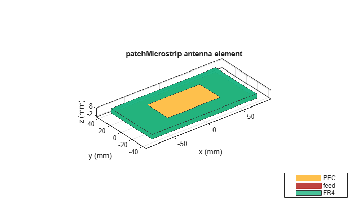
Create a PCB stack of this antenna.
pb = pcbStack(p);
Create an antenna design file using PCBWriter object.
s = PCBServices.GerbLookWriter;
s.Filename = 'patchM';
PW = PCBWriter(pb,s);
Set the default connector to false and write the antenna to a Gerber file.
PW.UseDefaultConnector = 0;
gerberWrite(PW)
Generated File: 'C:\Users\user\OneDrive - MathWorks\Documents\MATLAB\ExampleManager\user.Bdoc.DocWork0\antenna-ex33160284\patchM.zip'
'(name is available in system cut-buffer)

10 files in PCB stack
   Size Lines File
   126b    10 patchM.gtl (Copper,L1,Top,Signal)
   126b    10 patchM.gbl (Copper,L2,Bot,Signal)
    98b     9 patchM.gts (Soldermask,Top)
    98b     9 patchM.gbs (Soldermask,Bot)
   186k  9260 patchM.gto (Legend,Top)
     1k    34 patchM.gpi (PhotoplotterInfo,Info)
     1k    35 patchM.dri (DrillStationInfo,Info)
   237b    17 patchM.ipc (IPCD356A,Info)
    70k  3934 patchM.gbo (Legend,Bot)
              patchM.gml (Profile,NP)
Input Arguments
Output Arguments
Version History
Introduced in R2017b

