Create Antenna Model from Gerber Files
This example shows you how to create an antenna model from Gerber files and subsequently analyze the antenna. The Gerber file format is used in printed circuit board (PCB) manufacturing and is defined in the RS-274X standard which is the newer extended Gerber format. The Antenna Toolbox™ supports the newer RS-274X format both to generate Gerber files from an antenna model as well as to create an antenna model from a set of Gerber files.
Introduction
A set of Gerber files includes information about layer geometry, layer mask, solder paste usage on the layers, drill file and so on. To create a PCB antenna model out of these files, you need layer files that specify the antenna geometry, and if available a drill file to specify any plated through-hole (PTH) vias. The geometry of the layers is specified through either a top and bottom layer file, or a Gerber file. The Antenna Toolbox supports the Excellon format to specify drill information with file extensions .txt or .drl. To create an antenna model, import up to two layers and an optional drill file.
This example generates an antenna model using a single layer file and a two-layer file.
Import Single Layer Design and Analysis
While you can specify several antennas on a single side of a PCB, this example uses the design for an inverted-L antenna. The first step is to import a top-layer Gerber file into the workspace using the gerberRead function**.** This creates a PCBReader object. The PCBReader object provides access to the stackup that holds the information on the metal and dielectric layers and also any drill files that describe a PTH via from one metal layer to another. The GTL file that this example uses is held in the stackup as Layer2. If a second layer is present, you can specify it as Layer4 directly through the stackUp object or by passing it to the gerberRead function as the second input.
P1 = gerberRead('ILA_coplanar.gtl');
P1.StackUp
ans =
stackUp with properties:
NumLayers: 5
Layer1: [1×1 dielectric]
Layer2: 'ILA_coplanar.gtl'
Layer3: [1×1 dielectric]
Layer4: []
Layer5: [1×1 dielectric]
The PCBReader object also provides a property to control the discretization on any curved segments in the imported layer. The default value of this property, NumPointsOnCurves, is set to 50 in this example.
Model Creation
To create the antenna model, pass the PCBReader object as an input to the pcbStack object**.**
pb = pcbStack(P1);
figure
show(pb)
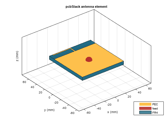
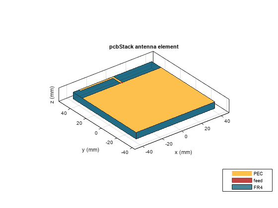
The Gerber file format does not provide information regarding a feed*.* The default feed is located at the origin in the created model. In order to make this model usable, modify the feed location on the layer.
pb.FeedDiameter = .001;
pb.FeedLocations(1:2) = [0,0.035];
figure
show(pb)
Import Two-Layer Design and Analysis
Import a two-layer design to create the antenna model. You can use the gerberRead function to create the PCBReader object. Pass in the top and bottom layers as inputs to the function.
P2 = gerberRead('UWBVivaldi.gtl','UWBVivaldi.gbl');
P2.StackUp
ans =
  stackUp with properties:

    NumLayers: 5
       Layer1: [1×1 dielectric]
       Layer2: 'UWBVivaldi.gtl'
       Layer3: [1×1 dielectric]
       Layer4: 'UWBVivaldi.gbl'
       Layer5: [1×1 dielectric]
Modify the third layer in the stack, which is the dielectric layer between the top and bottom metal layers.
S = P2.StackUp;
S.Layer3 = dielectric(Name="FR4", EpsilonR=4.4, Thickness=0.8e-3);
P2.StackUp = S;
Create the antenna model by passing pcbStack object as an input to the PCBReader object. Additionally, modify the feed information such as the coordinates, layer, and the diameter.
pb2 = pcbStack(P2);
pb2.BoardThickness = 0.8e-3;
pb2.FeedLocations=[-(44e-3/2), -(40e-3/2 - 11.2e-3 - 1.5e-3/2), 2, 4];
pb2.FeedDiameter = 1.5e-3/2;
figure
show(pb2)
axis equal;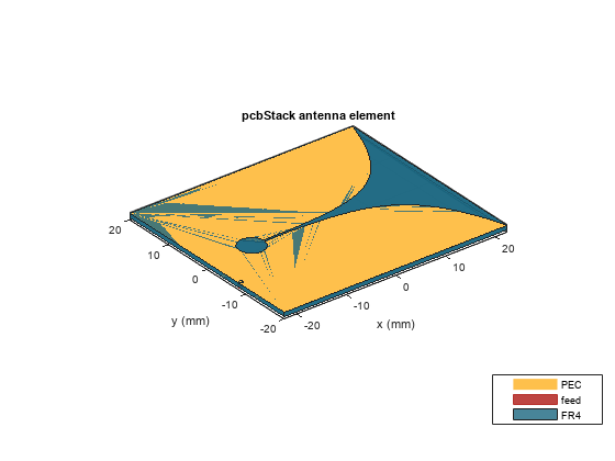
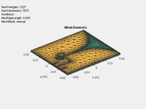
figure
mesh(pb2, MaxEdgeLength=5e-3, MinEdgeLength=0.8e-3);
Summary
Using the gerberRead function, you can create a PCBReader object, and subsequently use that object to generate the antenna model using a pcbStack object.
See Also
PCBReader | gerberRead | shapes | stackUp | Design, Analysis, and Prototyping of Microstrip-Fed Wide-Slot Antenna