PCBReader
R2026bImport PCB layout from stackup definition and drill files
Description
Use the PCBReader object to import a printed circuit board
(PCB) layout defined in a stackUp object and to facilitate the creation of
an antenna model. The layer files referenced by the stackup are Gerber files — a set of
manufacturing files that describe a PCB antenna. A Gerber file uses an ASCII vector format to
describe 2-D binary images. The object reads RS-274X Gerber files and does not support the
RS-274D format.
Creation
You can create a PCBReader object using either of these functions:
gerberRead— Import PCB layout directly from Gerber and drill files.PCBReader— Import PCB layout from astackUpdefinition object and drill files. This function is described here.
Description
B = PCBReader( creates a
S)PCBReader object that imports multilayer PCB antenna design files
described in the stackUp
object.
Note
To translate the center of an imported symmetrical or asymmetrical polygon to
[0,0] use the boundingbox and centroid
MATLAB® functions. For more information, see the examples section.
B = PCBReader( sets
properties
using one or more name-value arguments. PropertyName=Value)PropertyName is the property
name and Value is the corresponding value. You can specify several
name-value arguments in any order as PropertyName1=Value1,
..., PropertyNameN=ValueN. Properties that you
do not specify retain their default values. For example, B =
PCBReader(StackUp=S,DrillFile='ant.txt') imports the layers and drill file
into the PCBReader.
Input Arguments
Properties
Object Functions
shapes | Extract and modify metal layers from PCBReader
object |
Examples
Create a default PCB stackup definition object.
S = stackUp;
Set the thickness of the air dielectric layers 1 and 5 of the stackUp object to 0.1 mm.
S.Layer1.Thickness = 0.1e-3;
S.Layer5.Thickness = 0.1e-3;
Import a top layer Gerber file to layer 2.
S.Layer2 = "antenna_design_file.gtl";Import a bottom layer Gerber file to layer 4.
S.Layer4 = "antenna_design_file.gbl";Create a PCBReader object using the stackUp object.
B = PCBReader(StackUp=S);
Visualize the individual layers.
sh = shapes(B);
figure
show(sh(1))
title("Top Layer")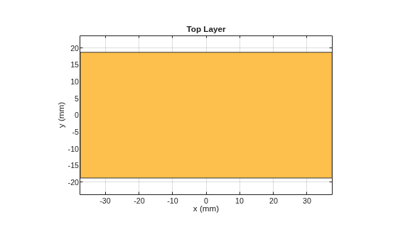
figure
show(sh(2))
title("Bottom Layer")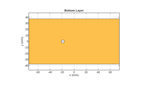
Create a default PCB stackup definition object.
s = stackUp;
Import a top layer Gerber file to layer 2.
s.Layer2 = "patchMicrostripCircular_design_file.gtl";Import a bottom layer Gerber file to layer 4.
s.Layer4 = "patchMicrostripCircular_design_file.gbl";Create a PCBReader object using the stackUp object.
p = PCBReader(StackUp=s);
To update the Gerber file, convert the PCBReader object to a pcbStack object.
p3 = pcbStack(p);
View the pcbStack object.
figure
show(p3)
title("Circular Patch Antenna")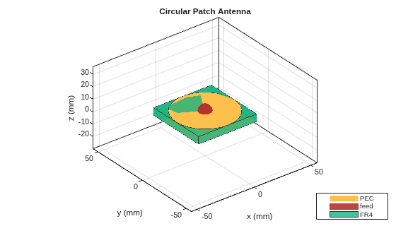
Update the feed locations and feed diameter.
p3.FeedLocations = [5e-3 0 2 4];
p3.FeedDiameter = 0.005;
View the updated pcbStack object.
figure
show(p3)
title("Circular Patch Antenna with Reduced Feed Diameter")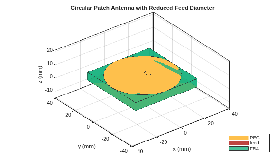
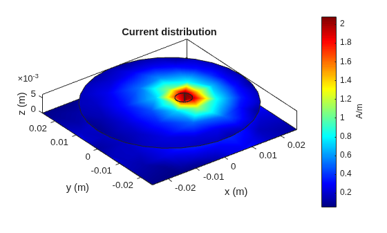
Plot the current distribution on the antenna at 2.4 GHz.
figure
current(p3,2.4e9)
Create a PCBReader object.
B = PCBReader;
Import a two-layer design.
st = B.StackUp;
st.Layer2 = "UWBVivaldi.gtl";
st.Layer4 = "UWBVivaldi.gbl";
B.StackUp = st;
Extract shapes from the metal layers.
S = shapes(B);
View the top-layer Gerber file.
figure
show(S(1))
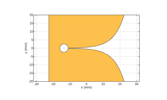
View the bottom-layer Gerber file.
figure
show(S(2))
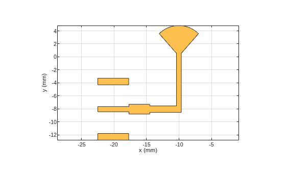
Create a PCB stackup object and import a rectangular patch to layer 2 and a dielectric to layer 3.
S = stackUp;
S.Layer2 = "PatchRectangular.gtl";
S.Layer3 = dielectric("Teflon");
Use a PCBReader object to read the PCB layout defined in the stackUp object. Visualize the shape of the PCB.
p1 = PCBReader(StackUp=S);
figure
show(p1.shapes)
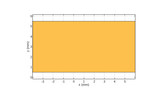
Translate the shape with center (0,0) using the centroid function from MATLAB.
s = p1.shapes
s =
  Polygon with properties:

        Name: 'mypolygon'
    Vertices: [4×3 double]
polygon = s;
[x,y] = centroid(polygon);
translate(polygon,[-x, -y, 0]);
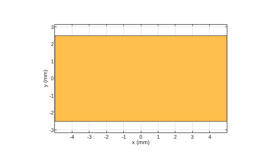
Create a PCB stackup object and import a rectangular patch to layer 2 and a dielectric to layer 3.
S = stackUp;
S.Layer2 = "RightAngleBend.gtl";
S.Layer3 = dielectric("Teflon");
Use a PCBReader object to read the PCB layout defined in the stackUp object. Visualize the shape of the PCB.
p1 = PCBReader(StackUp=S);
figure
show(p1.shapes)
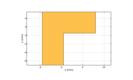
Translate the shape's bottom left corner to (0,0). Use the polyshape function to convert the shape to a polygon. Then, use the boundingbox function to compute the upper and lower bounds of the shape.
s = p1.shapes
s =
  Polygon with properties:

        Name: 'mypolygon'
    Vertices: [6×3 double]
ver = s.Vertices(:,1:2);
polygon = polyshape(ver);
[xlim, ylim] = boundingbox(polygon);
translate(s,[-xlim(1), -ylim(1), 0]);
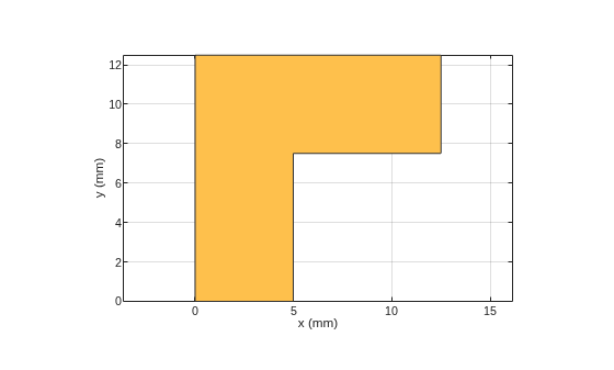
Create a stackUp object with three metal layers. Assign Gerber files to the metal layers.
s = stackUp(NumMetalLayers=3);
s.Layer2='TopLayer.gtl';
s.Layer4='InnerCopperLayer.g2l';
s.Layer6='BottomLayer.gbl'
s =
  stackUp with properties:

    NumMetalLayers: 3
         NumLayers: 7
            Layer1: [1×1 dielectric]
            Layer2: 'TopLayer.gtl'
            Layer3: [1×1 dielectric]
            Layer4: 'InnerCopperLayer.g2l'
            Layer5: [1×1 dielectric]
            Layer6: 'BottomLayer.gbl'
            Layer7: [1×1 dielectric]
Use the PCBReader object to import the PCB layout defined in the stackUp object. Specify the drill file and layer connectivity.
p = PCBReader(StackUp=s);
p.DrillLayerPairs = [1,3];
p.DrillFile = {'drillFile.txt'};
Convert the design into a PCB antenna using the pcbStack object. Define the feed properties.
pcbAnt = pcbStack(p);
pcbAnt.FeedDiameter = 0.5e-3;
pcbAnt.FeedLocations = [-5e-3 5e-3 2]
pcbAnt =
  pcbStack with properties:

              Name: 'TopLayer'
          Revision: 'v1.0'
        BoardShape: [1×1 antenna.Rectangle]
    BoardThickness: 0.0121
            Layers: {[1×1 dielectric]  [1×1 antenna.Polygon]  [1×1 dielectric]  [1×1 antenna.Polygon]  [1×1 dielectric]  [1×1 antenna.Polygon]  [1×1 dielectric]}
        FeedFormat: 'FeedLocations'
     FeedLocations: [-0.0050 0.0050 2]
      FeedDiameter: 5.0000e-04
      ViaLocations: [-0.0060 0.0071 2 6]
       ViaDiameter: 1.0000e-03
      FeedViaModel: 'square'
       FeedVoltage: 1
         FeedPhase: 0
         Conductor: [1×1 metal]
              Tilt: 0
          TiltAxis: [1 0 0]
              Load: [1×1 lumpedElement]
        SolverType: 'MoM'
Visualize the PCB antenna.
figure
show(pcbAnt)
title("PCB Antenna")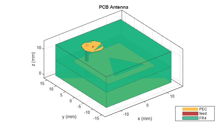
Version History
Introduced in R2020bSee Also
PCBWriter | PCBServices | PCBConnectors | pcbStack | stackUp | gerberRead

