gerberRead
R2026bCreate PCBReader object with specified Gerber and drill
files
Syntax
Description
P = gerberRead({M1,...,MN})PCBReader object with N metal layers. Each
M value specifies a Gerber file for a metal layer with layers ordered
based on their position in the cell array.
P = gerberRead({M1,...,MN},{D1,[fromLayer1,toLayer1];...;DN,[fromLayerN,toLayerN]})PCBReader object with metal layers and drill files. Each
D value specifies a drill file (.drl
or.txt). [fromLayer, toLayer] defines the
connection between the layers. This syntax supports specifying connections between
multiple vias and layers.
Examples
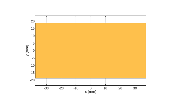
Use the gerberRead function to import a top layer Gerber file.
P = gerberRead("antenna_design_file.gtl");Extract the metal layer from the file using the shapes function.
s = shapes(P);
View the top metal layer.
show(s)
Import a bottom layer Gerber file to layer 4 of the stack.
P = gerberRead([],"UWBVivaldi.gbl");
P.StackUp
ans =
stackUp with properties:
NumMetalLayers: 2
NumLayers: 5
Layer1: [1×1 dielectric]
Layer2: []
Layer3: [1×1 dielectric]
Layer4: "UWBVivaldi.gbl"
Layer5: [1×1 dielectric]
Use the gerberRead function to import top and bottom layer Gerber files.
P = gerberRead("antenna_design_file.gtl","antenna_design_file.gbl");
Display the stack.
P.StackUp
ans =
  stackUp with properties:

    NumMetalLayers: 2
         NumLayers: 5
            Layer1: [1×1 dielectric]
            Layer2: "antenna_design_file.gtl"
            Layer3: [1×1 dielectric]
            Layer4: "antenna_design_file.gbl"
            Layer5: [1×1 dielectric]
Modify the third layer in the stack, which is the dielectric layer between the top and bottom metal layers.
S = P.StackUp;
S.Layer3 = dielectric(Name="FR4", EpsilonR=4.4, Thickness=0.8e-3);
P.StackUp = S;
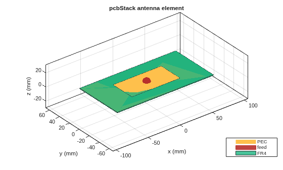
Create the antenna model by calling the pcbStack object on the PCB reader.
pb2 = pcbStack(P);
figure
show(pb2)
Import the design of a multilayer PCB antenna using Gerber and drill files.
g = gerberRead({'TopLayer.gtl','InnerCopperLayer.g2l','BottomLayer.gbl'},{'drillFile.txt',[2,3]})g =
PCBReader with properties:
StackUp: [1×1 stackUp]
DrillFile: {'drillFile.txt'}
DrillLayerPairs: [2 6]
NumPointsOnCurves: 50
View the information related to each layer.
g.StackUp
ans =
  stackUp with properties:

    NumMetalLayers: 3
         NumLayers: 7
            Layer1: [1×1 dielectric]
            Layer2: 'TopLayer.gtl'
            Layer3: [1×1 dielectric]
            Layer4: 'InnerCopperLayer.g2l'
            Layer5: [1×1 dielectric]
            Layer6: 'BottomLayer.gbl'
            Layer7: [1×1 dielectric]
Create an antenna from imported Gerber files using the pcbStack object.
p = pcbStack(g)
p =
  pcbStack with properties:

              Name: 'TopLayer'
          Revision: 'v1.0'
        BoardShape: [1×1 antenna.Rectangle]
    BoardThickness: 0.0121
            Layers: {[1×1 dielectric]  [1×1 antenna.Polygon]  [1×1 dielectric]  [1×1 antenna.Polygon]  [1×1 dielectric]  [1×1 antenna.Polygon]  [1×1 dielectric]}
        FeedFormat: 'FeedLocations'
     FeedLocations: [0 0 2]
      FeedDiameter: 0.0100
      ViaLocations: [-0.0060 0.0071 2 6]
       ViaDiameter: 1.0000e-03
      FeedViaModel: 'square'
       FeedVoltage: 1
         FeedPhase: 0
         Conductor: [1×1 metal]
              Tilt: 0
          TiltAxis: [1 0 0]
              Load: [1×1 lumpedElement]
        SolverType: 'MoM'
Change the feed diameter, set the feed location, and visualize the PCB antenna.
p.FeedDiameter = 0.5e-3;
p.FeedLocations = [-5e-3 5e-3 2]
p =
  pcbStack with properties:

              Name: 'TopLayer'
          Revision: 'v1.0'
        BoardShape: [1×1 antenna.Rectangle]
    BoardThickness: 0.0121
            Layers: {[1×1 dielectric]  [1×1 antenna.Polygon]  [1×1 dielectric]  [1×1 antenna.Polygon]  [1×1 dielectric]  [1×1 antenna.Polygon]  [1×1 dielectric]}
        FeedFormat: 'FeedLocations'
     FeedLocations: [-0.0050 0.0050 2]
      FeedDiameter: 5.0000e-04
      ViaLocations: [-0.0060 0.0071 2 6]
       ViaDiameter: 1.0000e-03
      FeedViaModel: 'square'
       FeedVoltage: 1
         FeedPhase: 0
         Conductor: [1×1 metal]
              Tilt: 0
          TiltAxis: [1 0 0]
              Load: [1×1 lumpedElement]
        SolverType: 'MoM'
figure
show(p)
title("PCB Antenna")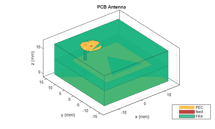
Read Gerber files and create a PCB design object. Extract and modify the stack-up by assigning a TMM4 dielectric, then update the PCB design.
g = gerberRead({"TopLayer.gtl","BottomLayer.gbl"});
s = g.StackUp;
s.Layer5 = dielectric('TMM4');
g.StackUp = s;
Convert the design to a PCB antenna using the pcbStack object.
p = pcbStack(g);
Visualize the PCB antenna.
figure
show(p)
title("Stacked Dielectric PCB Antenna")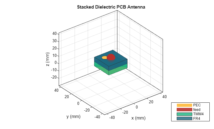
Input Arguments
Output Arguments
Limitations
Limitations of the gerberRead function while reading a
.gtl or .gbl file are:
| Command | Description | Comments |
| TF | File Attributes | Command is ignored and no error is thrown |
| TA | Aperture Attributes | Command is ignored and no error is thrown |
| TO | Object Attributes | Command is ignored and no error is thrown |
| TD | Delete Attributes | Command is ignored and no error is thrown |
Cut-ins are not supported.
Version History
Introduced in R2020bSee Also
shapes | PCBReader | PCBServices | PCBConnectors | PCBWriter

