Using I2C to Read and Write Data to Accelerometer on STM32 Processor Board
This example shows how to configure and use I2C Controller Read and Write blocks to get accelerometer data by using the Embedded Coder® Support Package for STMicroelectronics® STM32 Processors.
Required Hardware
To run this example, you need this hardware:
Reference Information
For information related to this example, see:
Configure Hardware Board
This example uses the LSM303AGR accelerometer, which is present on X-NUCLEO-IKS01A2 sensor expansion board. The sensor expansion board fits on STM32 Nucleo Arduino Uno compatible header as shown. Ensure that the sensor expansion board is installed correctly. With this setup,
I2C clock line (SCL) gets connected to PB8 (D15)
I2C data line (SDA) gets connected to PB9 (D14)
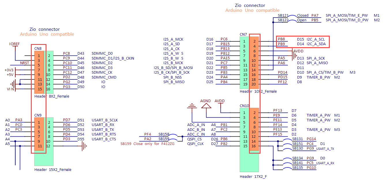
The X-NUCLEO-IKS01A2 is a sensor expansion board for the STM32 Nucleo, which comes with various sensors such as an accelerometer, a gyroscope, a magnetometer, a humidity sensor, a temperature sensor, a pressure sensor, and others. This example uses the LSM303AGR, which has a 3D accelerometer and a 3D magnetometer. Data is read from the 3-axis accelerometer over I2C protocol. For a brief overview of the sensors, study the data sheet.
The I2C protocol works with the main device initiating the start condition and sends a subordinate device address. Typically, the subordinate device address can be 7-bit or 10-bit and is mentioned in the sensor data sheet. Per the data sheet of the LSM303AGR, the default address for the I2C based accelerometer is 7-bit 0011001b.
SAD + read/write patterns
Command | SAD{6:0} | R/W | SAD + R/W |
|---|---|---|---|
Read | 0011001 | 1 | 00110011 (33h) |
Write | 0011001 | 0 | 00110010 (32h) |
Note: In the STM32 Embedded Coder I2C Controller read and write block, the R/W bit is managed by the driver block. For this reason, you should use 7-bit peripheral address (for example, 0011001b or 0x19).
Configure CTRL_REG1_A (0x20)
Use this register to configure:
Output Data Rate (ODR bits)
Operating mode (LPen bit along with HR bit in CTRL_REG4_A)
Enable/Disable individual axes. (Xen, Yen and Zen bits)
CTRL_REG1_A Bits
ODR3 | ODR2 | ODR1 | ODR0 | LPen | Zen | Yen | Xen |
CTRL_REG1_A Description
ODR[3:0] | Data rate selection. Default value: 0000 (0000: power-down mode; others: refer to data sheet) |
LPen | Enables low-power mode. Default value: 0 (0: normal mode, 1: low-power mode, others: refer to data sheet) |
Zen | Enables Z-axis. Default value: 1 (0: Z-axis disabled; 1: Z-axis enabled) |
Yen | Enables Y-axis. Default value: 1 (0: Y-axis disabled; 1: Y-axis enabled) |
Xen | Enables X-axis. Default value: 1 (0: X-axis disabled; 1: X-axis enabled) |
ODR[3:0] is used to set the power mode and ODR selection. This example uses a standard frequency of 100 Hz. To get that frequency, the example uses a value of ODR[3:0] as 0b0101.
Data Rate Configuration
ODR3 | ODR2 | ODR1 | ODR0 | Power mode selection |
|---|---|---|---|---|
0 | 0 | 0 | 0 | Power-down mode |
0 | 0 | 0 | 1 | HR / Normal / Low-power mode (1 Hz) |
0 | 0 | 1 | 0 | HR / Normal / Low-power mode (10 Hz) |
0 | 0 | 1 | 1 | HR / Normal / Low-power mode (25 Hz) |
0 | 1 | 0 | 0 | HR / Normal / Low-power mode (50 Hz) |
0 | 1 | 0 | 1 | HR / Normal / Low-poser mode (100 Hz) |
0 | 1 | 1 | 0 | HR / Normal / Low-poser mode (200 Hz) |
0 | 1 | 1 | 1 | HR / Normal / Low-power mode (400 Hz) |
1 | 0 | 0 | 0 | Low-power mode (1.620 kHz) |
1 | 0 | 0 | 1 | HR / Normal (1.344 kHz); Low-power mode (5.376 kHz) |
For selecting the operating mode, this example uses Normal Mode (output data is 10-bit). The LPen bit and HR bit (present in CTRL_REG4_A register) are kept to the default value of 0.
Operating Mode Selection
Operating mode | CTRL_REG1_A[3] (LPen bit) | CTRL_REG4_[3] (HR bit) | BW[Hz] | Turn-on time | So@1/-2 g [mg/digit] |
|---|---|---|---|---|---|
Low power mode (8-bit data output) | 1 | 0 | ODR/2 | 1 ms | 16 |
Normal mode (10-bit data output) | 0 | 0 | ODR/2 | 1.6 ms | 4 |
High resolution (12-bit data output) | 0 | 1 | ODR/9 | 7/ODR | 1 |
Not allowed | 1 | 1 | -- | -- | -- |
Configure CTRL_REG4_A (0x23)
Use this register to configure:
Endianess using BLE bit (this example uses Little Endian format, set by default value of 0)
Sensitivity using FS bits (this example uses sensitivity of 2g, set by default value of 0)
Operating mode (HR bit along with LPen bit in CTRL_REG1_A)
CTRL_REG4_A has a default value of 0.
CTRL_REG4_A Bits
BDU | BLE | FS1 | FS0 | HR | ST1 | ST0 | SPI_ENABLE |
Note: The BLE function can be activated only in high-resolution mode.
CTRL_REG4_A Description
BDU | Block data update. Default value: 0 (0: continuous update; 1: output registers not updated until MSB and LSB have been read) |
BLE | Big/little endian data selection. Default value: 0 (0: data LSb at lower address; 1: data MSb at lower address) The BLE function can be activated only in high-resolution mode. |
FS[1:0] | Full-scale selection. Default value: 00 (00: ±2 g; 01: ±4 g; 10: ± 8 g; 11: ±16 g) |
HR | Operating mode selection (refer to data sheet) |
ST[1:0] | Enables self-test. Default value: 00 (00: self-test disabled; other: refer to data sheet) |
SPI_ENABLE | Enables 3-wire SPI interface. Default: 0 (0: SPI 3-wire disabled; 1: SPI 3-wire enabled) |
Output Register Address for Accelerometer
This table shows register addresses, which are used to read the result of acceleration.
Accelerometer Output Register Addresses in Hexadecimal and Binary Format
Name | Hexadecimal | Binary |
|---|---|---|
OUT_X_L_A | 0x28 | 010 1000 |
OUT_X_H_A | 0x29 | 010 1001 |
OUT_Y_L_A | 0x2A | 010 1010 |
OUT_Y_H_A | 0x2B | 010 1011 |
OUT_Y_L_A | 0x2C | 010 1100 |
OUT_Y_L_A | 0x2D | 010 1101 |
Read Low and High Register Values of 3-Axis Accelerometer and Combine to Get 10-bit Output Data
In this example, the sensor is configured in Normal mode, the expected output is a 10-bit value. The 10-bit value are stored in two 8-bit registers. For example, X-axis has Low register (ex. OUT_X_L_A) and a High register (ex. OUT_X_H_A).
In this model, we will read both high and low register values and combine to get the 10-bit output value.
It is important to understand how data bytes are arranged in Low and High register. The figure shows the data-bit arrangement in high and low register. The I2C module is configured to operate in normal mode (output 10-bit data) and Little endian (data LSB at lower address). Also, data are stored left-justified in 8-bit output register. These data bits are stored in High and Low register as shown.
High Register
7 | 6 | 5 | 4 | 3 | 2 | 1 | 0 |
|---|---|---|---|---|---|---|---|
DB-9 | DB-8 | DB-7 | DB-6 | DB-5 | DB-4 | DB-3 | DB-2 |
Low Register
7 | 6 | 5 | 4 | 3 | 2 | 1 | 0 |
|---|---|---|---|---|---|---|---|
DB-1 | DB-0 | 0 | 0 | 0 | 0 | 0 | 0 |
The low register stores the two LSB of data at bit position six and seven and the rest of the bits remain 0. There can be four possible values, varying between zero (0b0000 0000), 64 (0b0100 0000), 128 (0b1000 0000), and 192 (0b1100 0000). The high register stores the MSB. When you rotate the sensor board, the acceleration difference can be noted in reading from this register.
To read the high and low registers, this example combines the data from both the registers.
The stm32_ex_i2c_read3AxisCombinedData model accomplishes this operation.
open_system('stm32_ex_i2c_read3AxisCombinedData');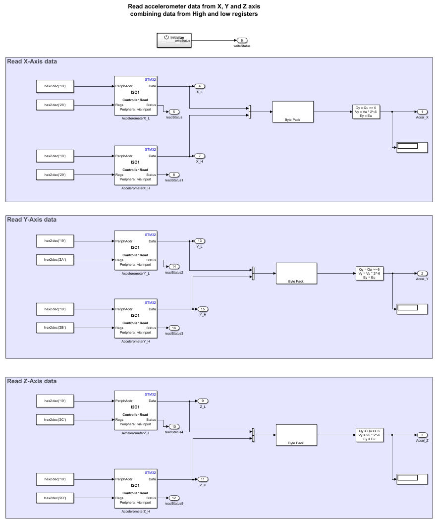
In this model, Vector Concatenate and Byte Pack blocks are used to merge the 8-bit data from High and Low registers into 16-bit. Because there are unwanted zeros in the Low register, the model right shifts 16-bit output by 6-bits to obtain the 10-bit data.
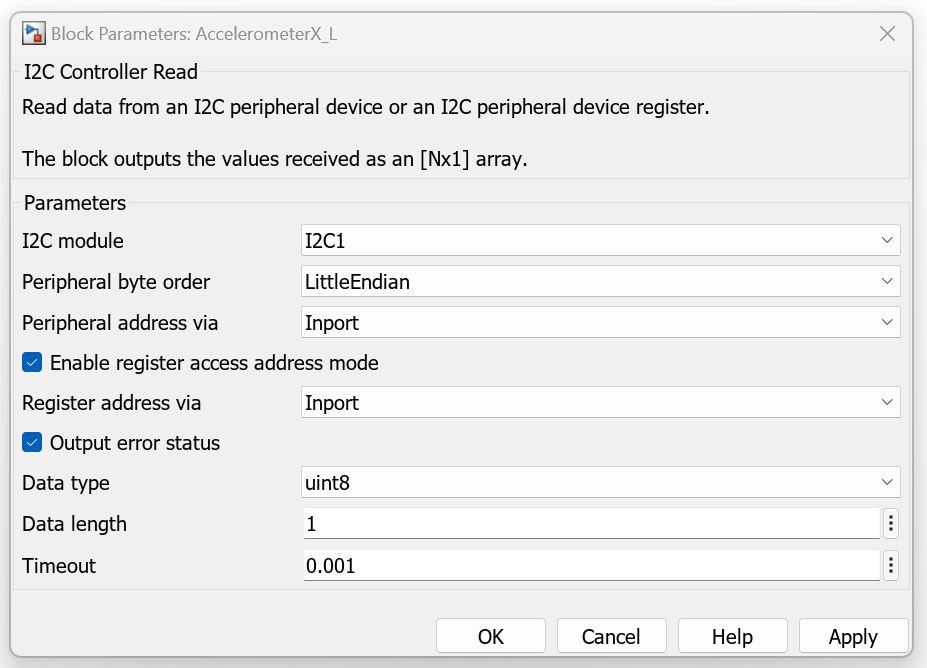
For I2C Controller Read block, set:
I2C module as I2C1
Peripheral byte order as LittleEndian
Peripheral address as 0x19
Select Enable register access address mode parameter. With this we enable the I2C register Read/Write mode. For more information, see Support I2C Communication and I2C operation section of data sheet.
Register address as 0x28. (Change it for axes as shown in the Accelerometer Output Register Addresses table)
Data type as uint8
Data length as 1
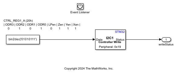
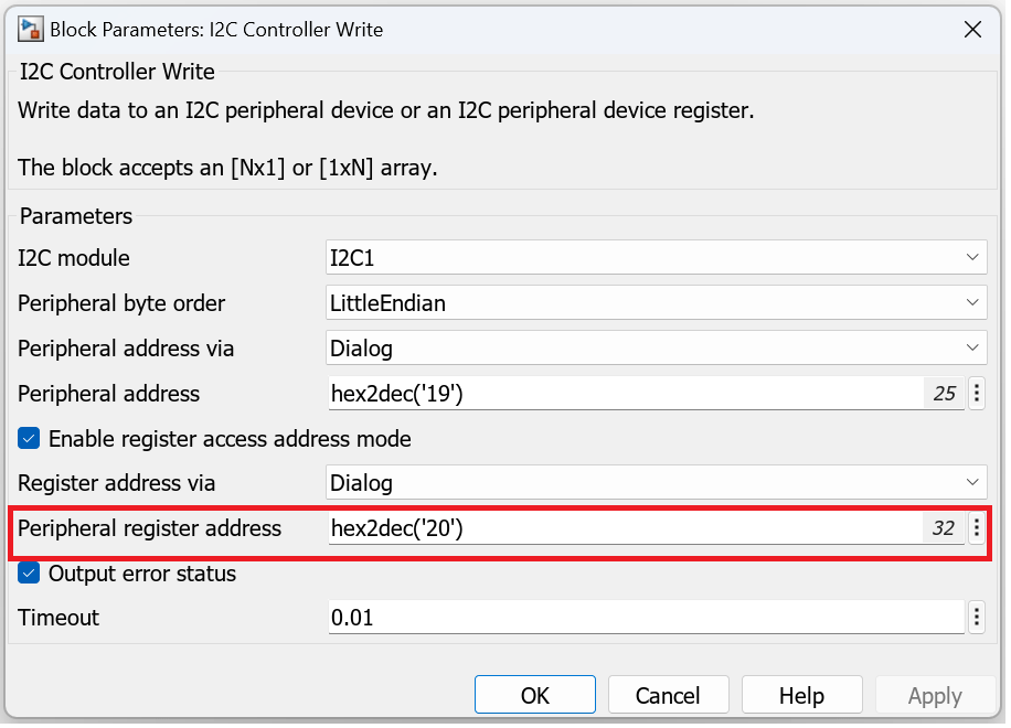
The model consists of an initialize subsystem, which is used to configure the control registers. The CTRL_REG1_A register is configured to set the correct ODR, operating mode, and enable the axes. The example uses the I2C controller Write block to write to CTRL_REG1_A (address: 0x20).
Configure STM32CubeMX
1. Open the Modeling tab and press CTRL+E to open the Configuration Parameters dialog box. Go to Hardware Implementation > Target Hardware Resources > Build options.
2. Click Browse. Browse for the stm32_i2c_gettingstarted.ioc file and click OK.
3. Click launch to open the IOC file.
4. Pin Configuration:
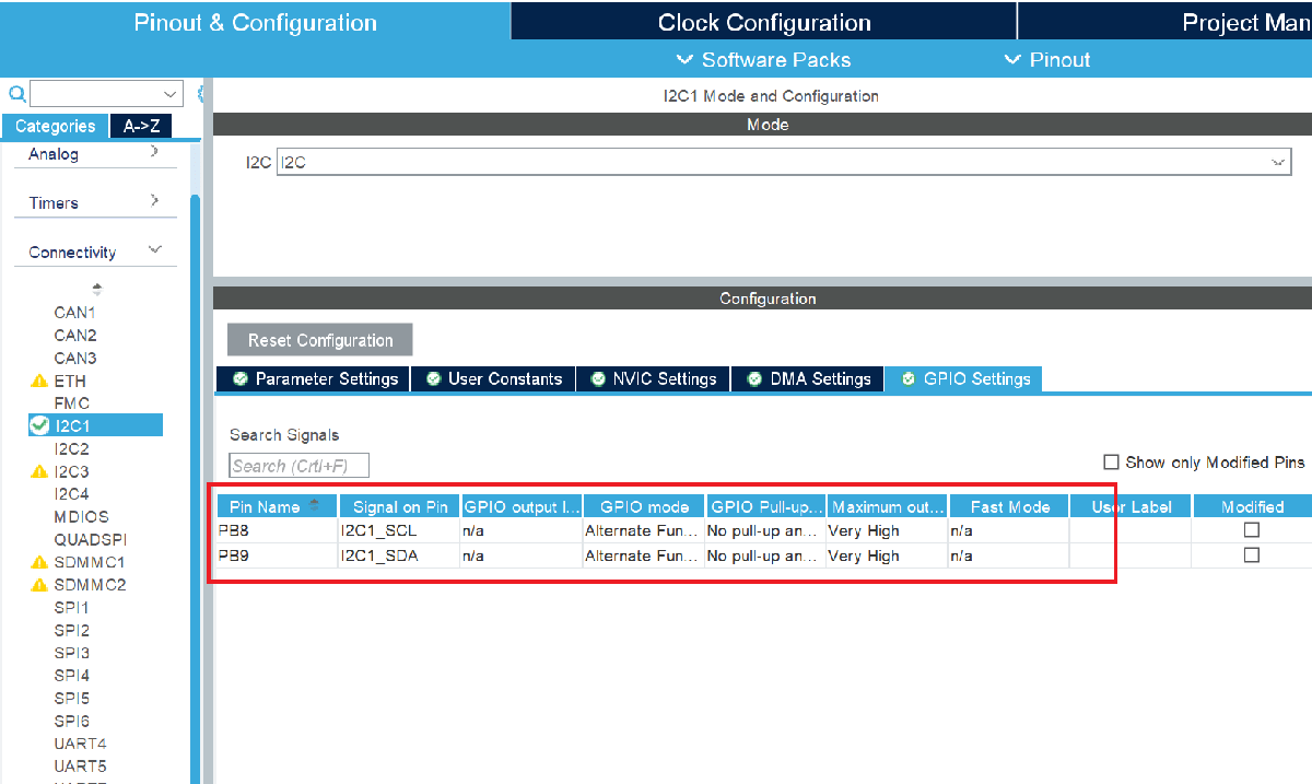
As we know from Configure Hardware board section, I2C clock line (SCL) is connected to PB8 pin. Navigate to STM32CubeMx and in Pinout view, search for pin number. Right click on highlighted pin and select I2C1_SCL to enable pin for SCL.
Similarly enable for pin PB9.
Note: As per sensor expansion board schematic, the SDA and SCL lines are pulled up with an external resistor. In case if these pull-up resistors are missing from sensor expansion board schematic, we should connect a pull up resistor. For calculation of resistor value refer Resistor value. For expansion board schematic, refer to Schematic diagram.

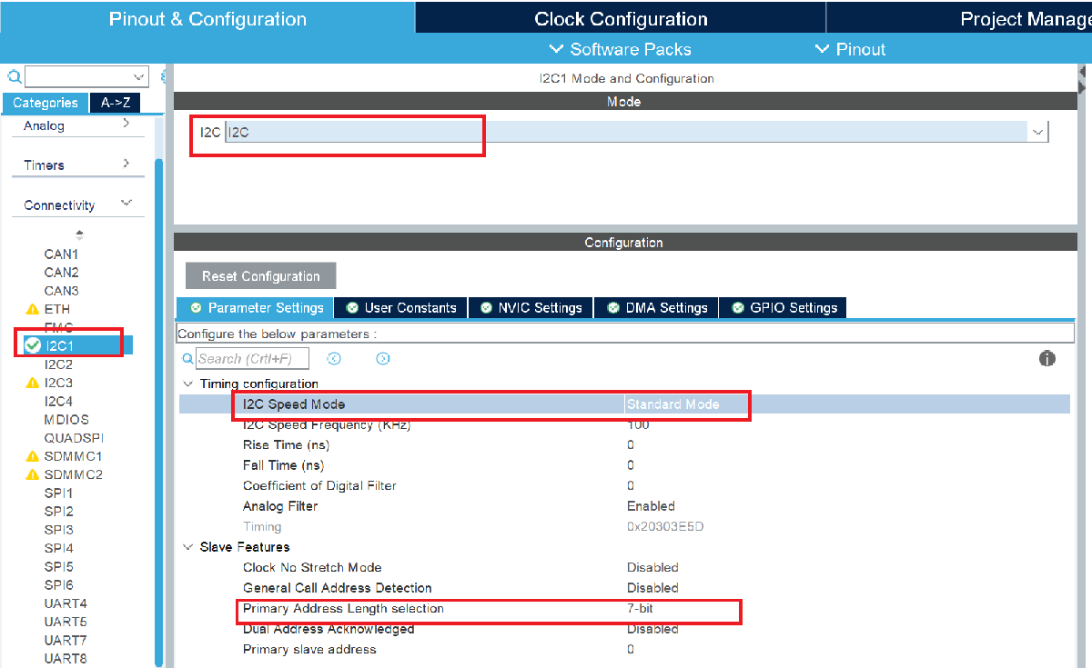
In the IOC file, Go to Pinout & Configuration > Connectivity > I2C1 and configure following settings.
Configure the IOC, to enable I2C. Ensure that I2C Speed Mode is set as Standard Mode, Primary Address Length selection is set as 7-bit.
5. Configure the model to run External Mode over serial by opening Hardware Implementation > Target Hardware Resources > Connectivity. For more information, see
6. Set USART/UART to USART3 (for STM32F767ZI nucleo board).
7. Set Serial port: COMx (where x: is com port number where Nucleo board is connected. You can get the com port information from Device Manager connected to Ports).
8. Click Apply and OK to close Configuration Parameters dialog box.
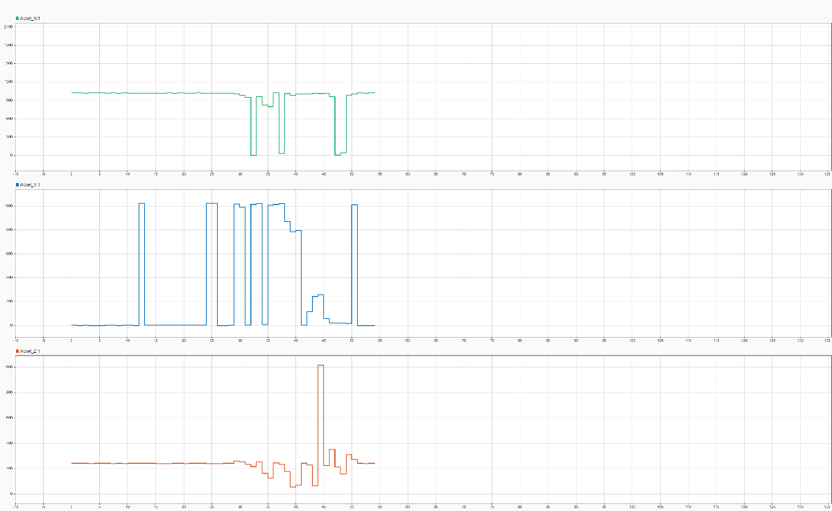
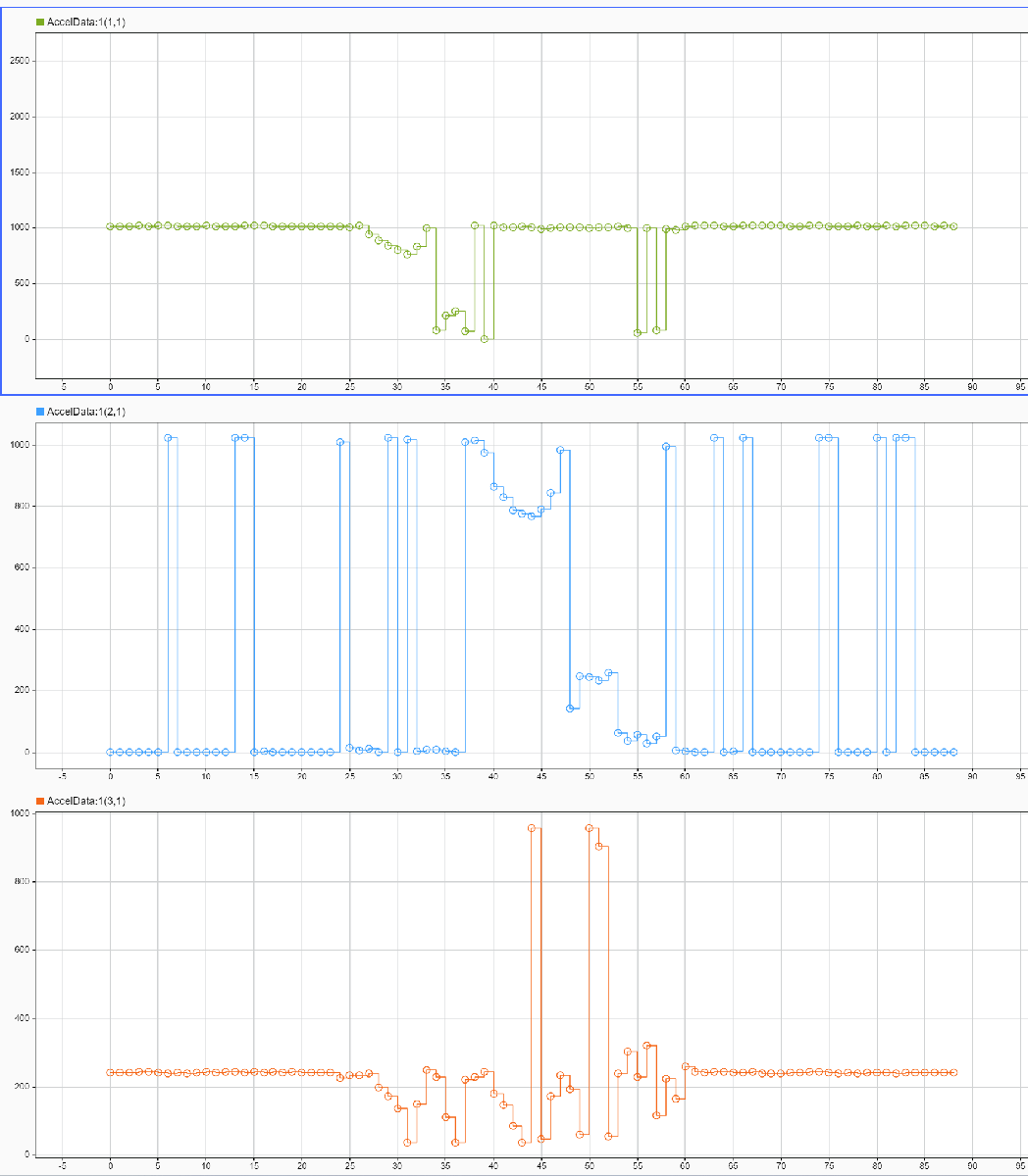
Click Monitor & Tune and verify the data using the Simulation Data Inspector.

Rotate the board and verify the data change in the Simulation Data Inspector.
AutoIncrement Register Address
In the Real Low and High Regiter Values of 3-Axis Accelerometer and Combine to Get 10-Bit Output Data section, the example models used one I2C Controller Read block for reading one register. With the LSM303AGR, it is also possible to read multiple bytes at a time. This example uses one I2C Controller Read block to read the results from the six output registers.
The example models in the previous sections used a 7-bit output register address. For example, the address for OUT_X_L_A is 0b010 1000(0x28). When the most significant bit (MSB) is set to 1. This setting enables the address to auto increment. The seven least significant bits represent the actual register address, while the most significant bit enables address auto increment.
The stm32_ex_i2c_read3AxisAutoIncrement model sets register address as 0b1010 1000 (0xA8), enabling auto increment. In this mode, the register address is automatically increased to allow reading of multiple bytes from consecutive memory address. Based on the number of bytes to be read, you set the data type and data length value in I2C controller read block.
For I2C Controller Read block, change:
Data type as uint16 (this groups result from low and high registers)
Data length as 3 (to read data from three axes.)
Register address as 0xA8
open_system('stm32_ex_i2c_read3AxisAutoIncrement');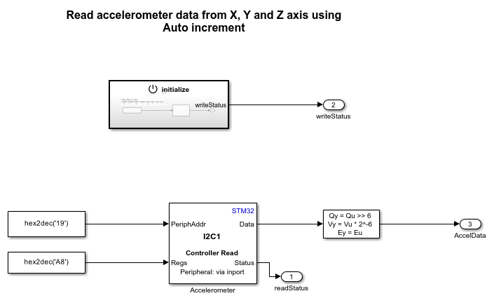
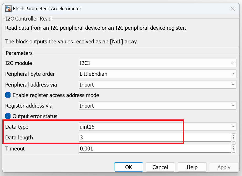
Click Monitor & Tune and verify the data using the Simulation Data Inspector. Rotate the board and verify the data change in the Simulation Data Inspector.
Measurement of Acceleration in g, Considering Linear Sensitivity for Accelerometer
To measure the acceleration in terms of g, it is important to consider the linear sensitivity of the accelerometer. The table shows full scale linear acceleration sensitivity. For more information, see the LSM303AGR data sheet. This example sets:
FS (full scale sensitivity) as ± 2g (from CTRL_REG4_A, FS bit, set as 0)
Normal mode (LPen bit in CTRL_REG1_A and HR bit in CTRL_REG4_A as 0)
Linear Sensitivity (mg/LSB)
FS = ±2 g and in high-resolution mode | -7% | 0.98 | +7% |
FS = ±4 g and in high-resolution mode | -7% | 1.95 | +7% |
FS = ±8 g and in high-resolution mode | -7% | 3.9 | +7% |
FS = ±16 g and in high-resolution mode | -7% | 11.72 | +7% |
FS = ±2 g and in normal mode | -7% | 3.9 | +7% |
FS = ±4 g and in normal mode | -7% | 7.82 | +7% |
FS = ±8 g and in normal mode | -7% | 15.63 | +7% |
FS = ±16 g and in normal mode | -7% | 46.9 | +7% |
FS = ±2 g and in low-power mode | -7% | 15.63 | +7% |
FS = ±4 g and in low-power mode | -7% | 31.26 | +7% |
FS = ±8 g and in low-power mode | -7% | 62.56 | +7% |
FS = ±16 g and in low-power mode | -7% | 187.58 | +7% |
The stm32_ex_i2c_LinearSensitivity model sets:
Linear sensitivity as 3.9 mg/LSB
Gain factor = (3.9/1000)*9.8 g (to put acceleration in terms of g)
open_system('stm32_ex_i2c_LinearSensitivity');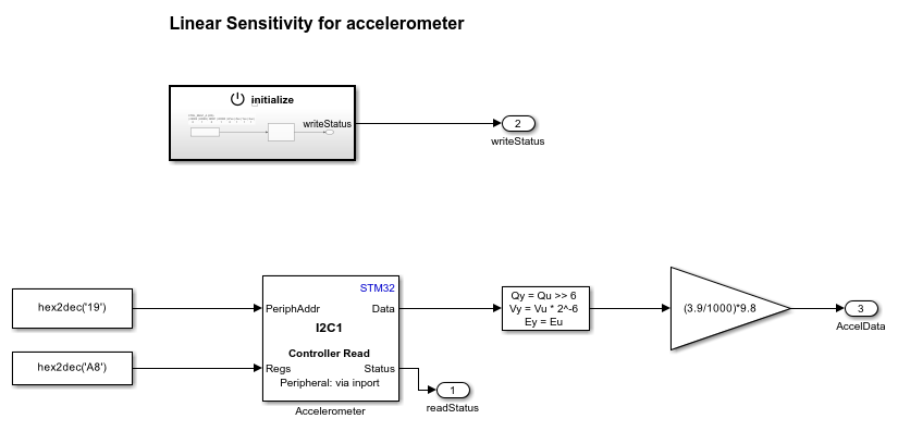
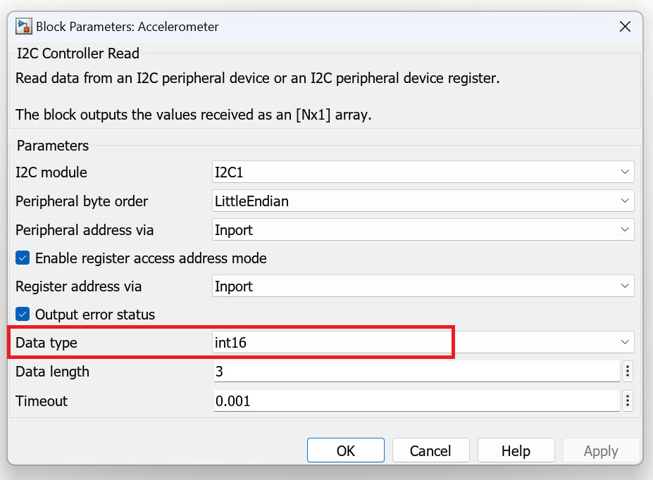
For I2C Controller Read block, change:
Data type as int16 (to measure accelerometer in terms of +- g)
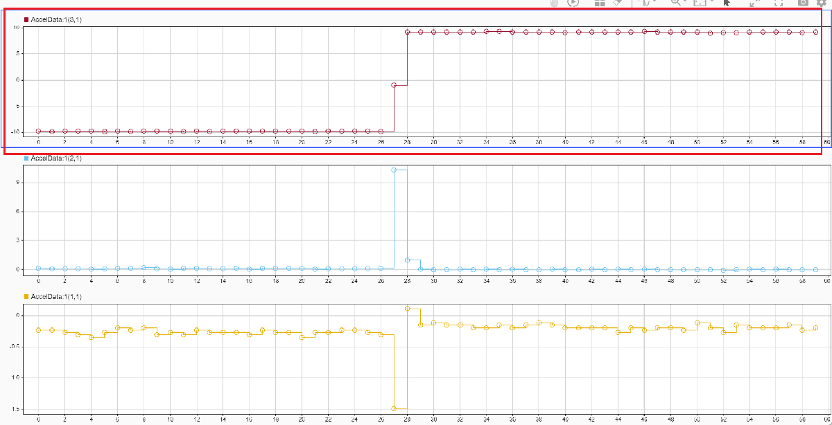
Click Monitor & Tune and verify the data using the Simulation Data Inspector. The figure shows the Z-axis acceleration in terms of g (marked in red box). Make sure to keep the board on a flat table facing upward (sensor facing sky). In this case, you should get a reading approximately equal to positive g or +9.8. Then, flip the board upside-down (sensor should face earth), Now, you should see acceleration as negative g or -9.8.
Other Things to Try
Read data in big endian format by setting bits in CTRL_REG4_A and Peripheral byte order in I2C Read block mask. Build understanding on data byte arrangement and combine result of both registers.
Read data when it is available by using in interrupt line for accelerometer. Refer to sensor datasheet for details.
Close All Opened Models
bdclose('stm32_ex_i2c_read3AxisCombinedData');
bdclose('stm32_ex_i2c_read3AxisAutoIncrement');
bdclose('stm32_ex_i2c_LinearSensitivity');