Block Generation with the FIL Wizard
Step 1: Set Up FPGA Design Software Tools
Step 2: Start FIL Wizard
Open the FPGA-in-the-loop wizard by selecting one of the following invocation methods:
In the MATLAB command window, type the following:
>> filWizard
In the Simulink® toolstrip, on the Apps tab, under Code Verification, Validation and Test click FIL Wizard.
To restore a previous session, use this command:
filWizard('./Subsystem_fil/Subsystem_fil.mat')Step 3: Set FIL Options for FIL Block

On the FIL Options page:
FIL Simulation: Select
Simulink.Board Name: Select an FPGA development board. If you have not yet downloaded an HDL Verifier™ FPGA board support package, see Download FPGA Board Support Package. (If you do not see any boards listed, then you have not yet downloaded a support package). If you plan to define a custom board yourself, see FPGA Board Customization.
FPGA-in-the-Loop Connection: Select the FIL simulation connection method. The options in the drop-down menu update depend on the connection methods supported for the target board you selected. If the target board and HDL Verifier support the connection, you can choose
Ethernet,JTAG,PCI Express, orUSB Ethernet.Advanced Options:
When you select an Ethernet connection for an FPGA board, you can adjust the board IP and MAC addresses, if necessary. If the board includes a processing unit, use the Guided Hardware Setup to configure the SD card.
Option Instructions Board IP address Use this option for setting the IP address of the board if it is not the default IP address (192.168.0.2).
If the default board IP address (192.168.0.2) is in use by another device, or you need a different subnet, change the Board IP address according to the following guidelines:
The subnet address, typically the first three bytes of board IP address, must be the same as the subnet of the host IP address.
The last byte of the board IP address must be different from the last byte of the host IP address.
The board IP address must not conflict with the IP addresses of other computers.
For example, if the host IP address is 192.168.8.2, then you can use 192.168.8.3, if available.
Board MAC address Under most circumstances, you do not need to change the board MAC address. If you connect more than one FPGA development board to a single host computer, change the board MAC address for any additional boards so that each address is unique. You must have a separate NIC for each board.
To change the Board MAC address, click in the Board MAC address field. Specify an address that is different from that belonging to any other device attached to your computer. To obtain the Board MAC address for a specific FPGA development board, refer to the label affixed to the board or consult the product documentation.
FPGA system clock frequency (MHz): Enter a target clock frequency. For Intel boards and AMD ISE-supported boards,
filWizardchecks the requested frequency against those possible for the requested board. If the requested frequency is not possible for this board,filWizardreturns an error and suggests an alternate frequency. For AMD Vivado-supported boards, or PCI Express® boards,filWizardcannot check the frequency. The synthesis tools make a best effort attempt at the requested frequency but may choose an alternate frequency if the specified frequency was not achievable. The default is25MHz.Enable data buffering on FPGA: Select this option to enhance simulation performance. When selected, FIL utilizes BRAMs on the FPGA to buffer Ethernet packets in frame-based processing mode. Clear this parameter when BRAM resources are scarce in your design. Available for Ethernet connection only.
Click Next.
Step 4: Add HDL Source Files for FIL Block
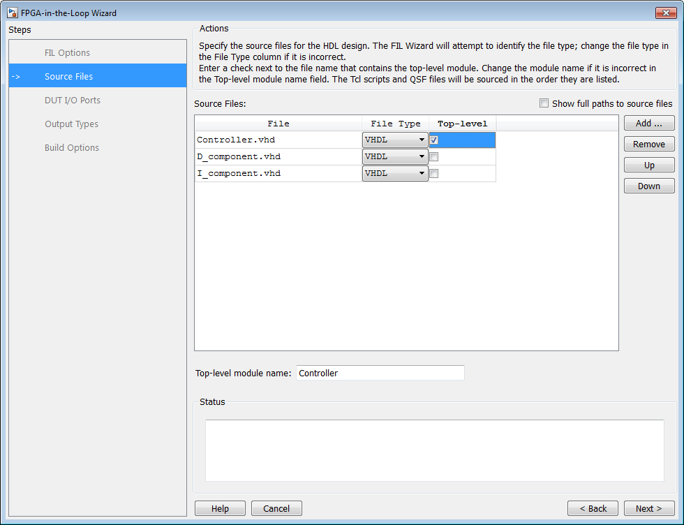
On the Source Files page:
Specify the HDL design to be cosimulated in the FPGA. These files are the HDL design files to be verified on the FPGA board.
Indicate source files by clicking Add. Select files using the file selection dialog box.
The FIL wizard attempts to identify the source file types. If any of the file types is not what you expect, you can change it by selecting from the File Type drop-down list. Acceptable file types are:
VHDL®
Verilog®
SystemVerilog
Netlist
Tcl script
Constraints
Others
"Others" refers to the following:
For Intel, files specified as
Otherare added to the FPGA project, but they have no impact on the generated block. For example, you can put some comments in areadmefile and include it in this file list.For AMD, files specified as
Othercan be any file accepted by AMD ISE. ISE looks at the file extension to determine how to use this file. For example, if you addfoo.vhdto the list and specify it asOther, ISE treats the file as a VHDL file.
Specify which file contains the top-level HDL file.
Check the box on the row of the HDL file that contains the top-level HDL module in the column titled Top-level. The FIL wizard automatically fills the Top-level module name field with the name of the selected HDL file. If the top-level module name and file name do not match, you can manually change the top-level module name in this dialog box. Indicate the top-level module name before you continue.
(Optional) To display the full paths to the source files, check the box titled Show full paths to source files.
Click Next.
Step 5: Verify DUT I/O Ports for FIL Block
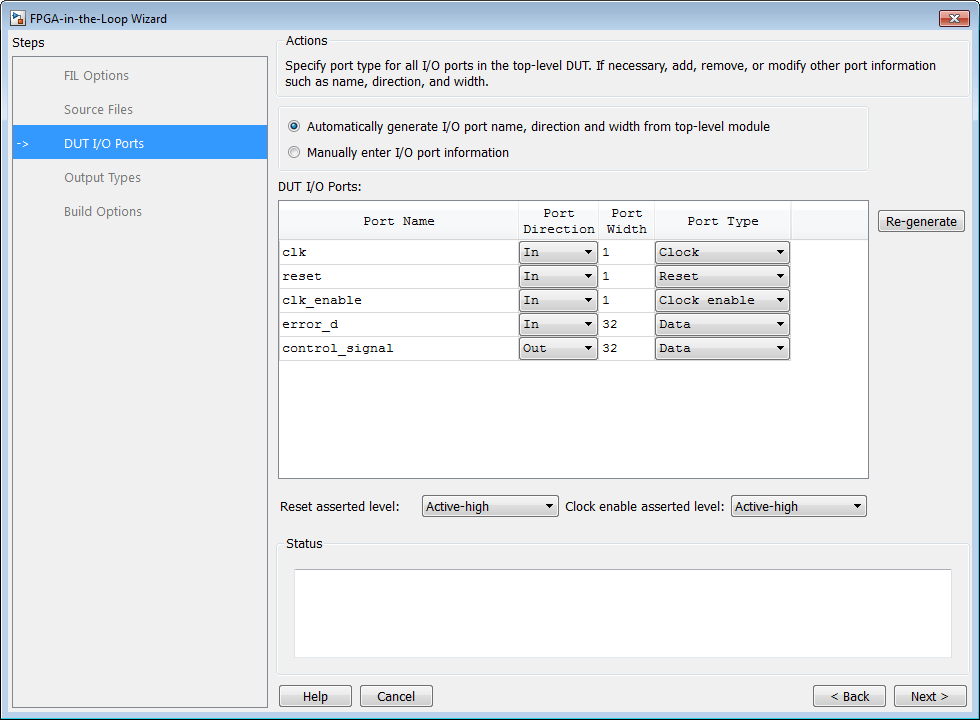
On the DUT I/O Ports page:
Review the port listing. The FIL wizard parses the top-level HDL module to obtain all the I/O ports and display them in the DUT I/O Ports table. The parser attempts to determine the port types from the port names. The wizard then displays these signals under Port Type. Select from:
ClockResetClock enableDataStreaming data– available when Synchronization Mode is set toFree-running FPGA.Streaming valid– available when Synchronization Mode is set toFree-running FPGA.Streaming ready– available when Synchronization Mode is set toFree-running FPGA.Control data– available when Synchronization Mode is set toFree-running FPGA.
Make sure all input/output/reset ports/clocks are mapped as you expect. If the parser assigned an incorrect port type for any port, you can manually change the signal. For synchronous design, specify a Clock, Reset, or, if desired, a Clock enable signal. The port types specified in this table must be the same as in the HDL code. There must be at least one output port.
Select Manually enter port information to add or remove signals.
Click Regenerate to reload the table with the original port definitions (from the HDL code).
Click Next.
Step 6: Specify Output Types for FIL Block
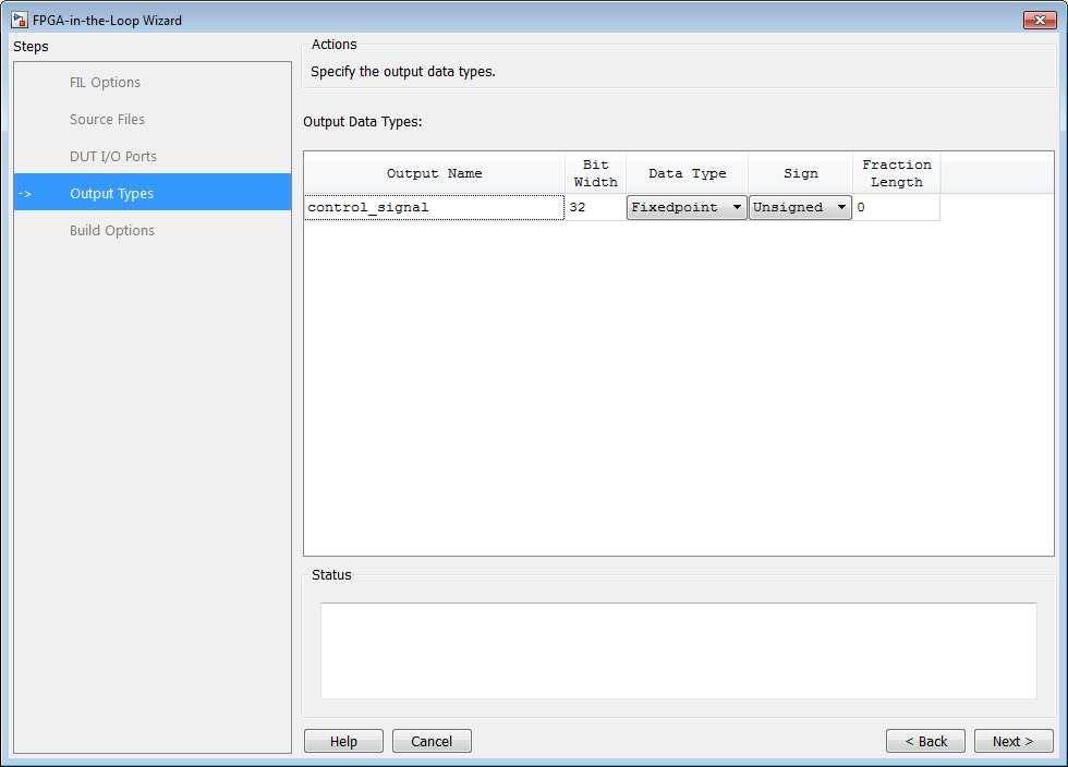
On the Output Types page:
Specify output data types. The wizard assigns data types. If any output data type is not what you expect, manually change the type.
Select from:
FixedpointIntegerLogical
The data type can depend on the specified bit width.
You can specify the output type to be
Signed,Unsigned, orFraction Length.Click Next.
Step 7: Specify Build Options for FIL Block
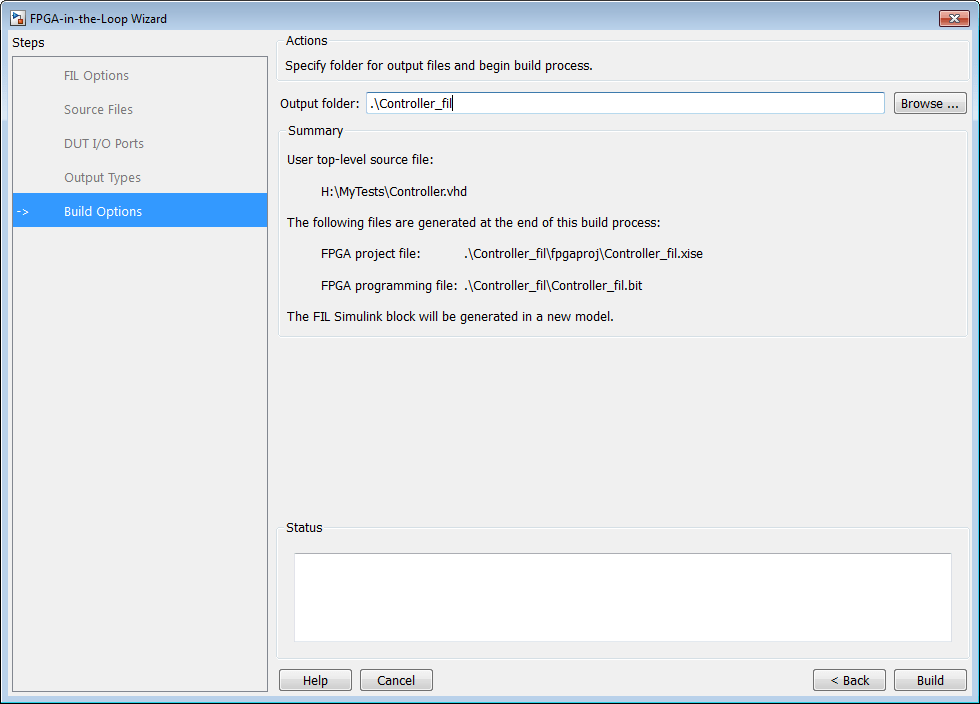
On the Build Options page:
Specify the folder for the output files. You can use the default option. Usually the default is a subfolder named after the top-level module, located under the current folder.
Note the locations of the ISE project file and the FPGA programming file in the Summary. You may need those two files for advanced operations on the FIL block mask.
Step 8: Initiate Build
Click Build to initiate FIL block generation.
The FIL wizard generates a FIL block named after the top-level module and places it in a new model.
The FIL wizard opens a command window.
In this window, the FPGA design software performs synthesis, fit, PAR, and FPGA programming file generation.
When the process completes, a message in the command window prompts you to close the window.

Step 9: Integrate and Simulate
Insert FIL Block Into Model
In your model, replace the DUT subsystem with the FIL block generated in the new model. Save the model under a different name. You can then use the original model as a reference model.
If you generated your FIL block from the HDL workflow advisor, it is unlikely that you need to adjust any settings on the FIL block. If you generated your FIL block using the FIL wizard, you may want to adjust some settings. For instructions on adjusting the FIL block settings, see FIL Simulation.
Load Programming File onto FPGA
![]() Intel Board Instructions for Linux
Intel Board Instructions for Linux
Ensure that your FPGA development board is set up, turned on, and connected to your machine using a JTAG cable. Programming uses the JTAG interface, even if you select a different connection for simulation.
Perform the following steps to program the FPGA:
Double-click the FIL block in your Simulink model to open the block mask.
On the Main tab, click Load to download the programming file to the FPGA via the JTAG cable.
The load process can take from a few minutes to several minutes or longer, depending on how large the subsystem is. Sometimes, the process can take an hour and a half or longer for large subsystems.
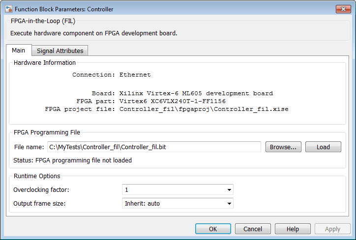
A message window indicates when the FPGA programming file has loaded as expected. Click OK.
Run Simulation
In Simulink, run the model that includes the FIL Simulation block. The results of the FIL simulation should match the results of the Simulink reference model or of the original HDL code.
Note
RAM Initialization: Simulink starts from time 0 every time, which means the RAM in a Simulink model is initialized to zero for each run. However, this assumption is not true in hardware. RAM in the FPGA holds its value from the end of one simulation to the start of the next. If you have RAM in your design, the first simulation matches Simulink, but subsequent runs may not match. The workaround is to reload the FPGA bitstream before rerunning the simulation. To reload the bitstream, click the Load on the FIL block mask.