PCI Express AXI Manager
Note
PCI Express® AXI master has been renamed to PCI Express AXI manager and the PCIe MATLAB® as AXI Master IP has been renamed to the PCIe AXI Manager IP. In the software and documentation, the terms "manager" and "subordinate" replace "master" and "slave," respectively.
When using PCI Express AXI manager, you must first include the following two intellectual property (IP) blocks in your AMD® Vivado® project.
PCIe AXI Manager IP
PCI Express Core
PCIe AXI Manager IP
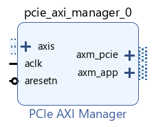
PCIe AXI Manager is an HDL IP provided by MathWorks®. This IP connects the PCI Express (PCIe) core to your application code. The IP has a configuration port for accessing configuration registers. This block diagram shows the interface to the HDL IP. To know how to include the PCIe AXI Manager IP in your FPGA design, see Set Up AXI Manager.

The interface includes the following parts:
clockandresetnare the clock and reset inputs. Connect them to the AXI clock and reset.axs_s0is a 32-bit subordinate interface and is used for accessing the PCIe configuration registers. Connect this interface to the Kintex® UltraScale+™ FPGA KCU116 memory mapped manager interface.axm_pcieis a 128-bit AXI manager interface. Connect this interface to the S_AXI_B subordinate port on the PCIe core.axm_appis a 128-bit AXI manager interface. Connect this interface to your application logic.
After instantiating this IP in your design, open the block parameters for configuration.

Configure these parameters:
AXI Address Width – This parameter is the address bus width. The IP supports 32-bit address.
AXI Data Width – This parameter is the data bus width. The IP supports only 128-bit. Note that this parameter is not identical to the data width of the
aximanagerobject or the AXI Manager Read or AXI Manager Write blocks. If the data width is set to 32 bits, and the AXI Data Width of your IP is set to 128 bits, HDL Verifier™ packs four 32-bit words to transfer on the 128-bit bus.ID Width – This parameter is the ID width in bits. Its value must match the ID width of the AXI subordinate.
PCI Express Core
The DMA/Bridge Subsystem for PCI Express Core is a board-specific IP provided by AMD. Use this IP for configuring and integrating the PCI Express port. For more information on how to include this IP in your FPGA design, see Set Up AXI Manager.
After instantiating the PCIe core HDL IP in your AMD Vivado project, configure the PCIe core using these steps. This example is for a Kintex UltraScale+ FPGA KCU116 board.
On the Basic tab, set the parameters as shown in this figure.

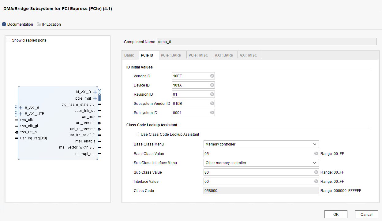
On the PCIe ID tab, set the parameters as shown in this figure.

The ID Initial Values listed in the PCIe tab screen are the required PCIe ID settings to ensure compatibility with MathWorks PCIe device driver for AMD FPGA boards.
Connect the PCIe AXI Manager IP to the PCIe core. This example shows the Kintex UltraScale+ FPGA KCU116 DMA/Bridge Subsystem IP for PCI Express.

Compile and build your FPGA project.
Insert the FPGA board into the PCI Express slot on the motherboard of the host machine.
Program FPGA with the bitstream generated for your design.
Restart the host machine.
Once the program is running on your FPGA board, you can create an AXI manager
object in your MATLAB command window. For more information, see aximanager. To access the subordinate memory locations on the board,
use the readmemory and writememory functions of this object.