Modeling and Testing an LTE RF Transmitter
This example shows how to characterize the impact of radio frequency (RF) impairments, such as in-phase and quadrature (IQ) imbalance, phase noise, and power amplifier (PA) nonlinearities, on the performance of an LTE transmitter. The example generates the baseband LTE waveform, which consists of an E-UTRA test model (E-TM), by using LTE Toolbox™ software and models the RF transmitter by using RF Blockset™ software.
Introduction
This example characterizes the impact of RF impairments such as in-phase and quadrature imbalance, phase noise, and power amplifier nonlinearities on the performance of an LTE RF transmitter. To evaluate the performance, the example performs these measurements:
Error vector magnitude (EVM): vector difference at a given time between the ideal (transmitted) signal and the measured (received) signal. The example performs EVM measurements according to the specifications in TS 36.104, Annex E.
Occupied bandwidth: bandwidth that contains 99% of the total integrated power of the signal, centered on the assigned channel frequency
Channel power: filtered mean power centered on the assigned channel frequency
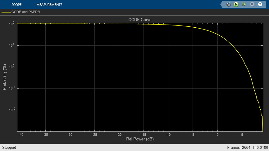
Complementary cumulative distribution function (CCDF): probability that the signal's instantaneous power is at a specified level above its average power
Peak-to-average power ratio (PAPR): relation between the peak power of the signal and its average power
The example works on a subframe-by-subframe basis and uses a Simulink® model to perform these steps:
Generate the baseband E-TM waveform using LTE Toolbox functions.
Import the baseband waveform into the RF Transmitter Subsystem block implemented by using RF Blockset blocks. The model uses an RF intermediate frequency to carry the baseband information in RF Blockset.
Model the effects of upconverting the waveform to the carrier frequency by using the RF Transmitter Subsystem block. This block models the impairments introduced by an RF transmitter using RF Blockset blocks.
Calculate the occupied bandwidth and the channel power by using the Spectrum Analyzer block.
Compute the CCDF and PAPR.
Extract the data symbols and measure the EVM by demodulating the baseband waveform.
The Simulink model uses LTE Toolbox and DSP System Toolbox™ features to process the baseband signal (steps 1, and 4-6) and uses RF Blockset blocks to model the RF transmitter (steps 2 and 3). This model supports Normal and Accelerator simulation modes.
Simulink Model Structure
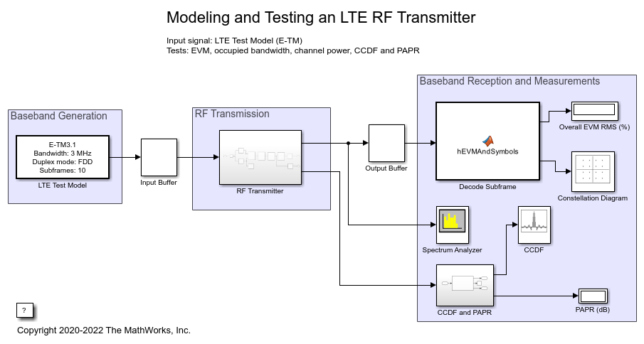
The model contains three main parts:
Baseband Waveform Generation: generates the baseband E-TM waveforms
RF Transmission: models the effects of upconverting the waveform to the carrier frequency
Baseband Reception and Measurements: performs the RF measurements and calculates EVM by demodulating the baseband waveform
modelName = 'RFLTETransmitterModel';
open_system(modelName);
Baseband Generation
The LTE Test Model block transmits a standard-compliant LTE test model 3.1 (E-TM3.1) waveform, as defined in TS 36.141. This block is generated using the LTE Waveform Generator app. You can access the waveform configuration parameters in the user data of the block. This example uses the InitFcn in the Model callbacks to store the structure available in the user data in a Base Workspace variable, LTEInfo. For more information about this block, see Waveform From Wireless Waveform Generator App.
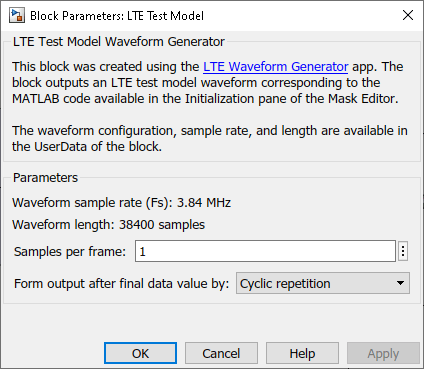
To use a different E-TM waveform, open the LTE Waveform Generator app, select the E-TM configuration, and export a new block. For more information on how to generate and use this block, see Generate Wireless Waveform in Simulink Using App-Generated Block.
RF Transmission
The RF Transmitter Subsystem block is based on a superheterodyne transmitter architecture. This architecture models the effects of upconverting the waveform to the carrier frequency by characterizing these RF components:
IQ modulator consisting of mixers, a phase shifter, and a local oscillator
Bandpass filter
Power amplifier
In addition to these components, this RF Transmitter Subsystem block also includes a variable gain amplifier (VGA) to control the input back-off (IBO) level of the high power amplifier (HPA).
set_param(modelName,'Open','off');
set_param([modelName '/RF Transmitter'],'Open','on');
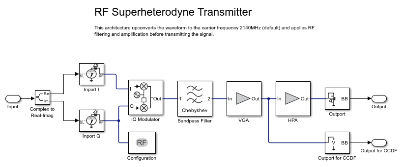
Use an Input Buffer block to send one sample at a time to the RF Transmitter Subsystem block.
The Inport block inside the RF Transmitter Subsystem block converts the Simulink complex baseband waveform into the RF Blockset Circuit Envelope simulation environment. The Carrier frequencies parameter of the Inport block specifies the center frequency of the carrier in the RF Blockset domain. The Outport block converts the RF Blockset signal back into Simulink complex baseband.
You can configure the RF Transmitter components using the RF Transmitter Subsystem block mask.
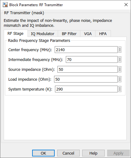
The RF Transmitter Subsystem block models typical impairments, including:
I/Q imbalance as a result of gain or phase mismatches between the parallel sections of the transmitter chain dealing with the IQ signal paths.
Phase noise as a secondary effect directly related to the thermal noise within the active devices of the oscillator.
HPA nonlinearities due to DC power limitation when the amplifier works in saturation region.
Before sending the samples onto the Decode Subframe block, the Output Buffer (after the RF Transmitter) collects all samples within a subframe.
The use of buffers in the model generates time delays. As the duration of the delay is equivalent to the transmission of a subframe, the Decode Subframe block does not demodulate the first subframe.
Baseband Reception and Measurements
The Decode Subframe block performs OFDM demodulation of the received subframe, channel estimation, and equalization to recover and plot the PDSCH symbols in the Constellation Diagram. This block also performs EVM measurements according to the specifications in TS 36.104, Annex E. These specifications suggest measuring the EVM at two locations in time (low and high), where the low and high locations correspond to the alignment of the FFT window within the start and end of the cyclic prefix, respectively. For more information regarding how to measure EVM, see PDSCH Error Vector Magnitude (EVM) Measurement.
This example carries out EVM measurements averaged over the allocated PDSCH symbols within a subcarrier, resource block, OFDM symbol, subframe, frame, and overall grid. The EVM per subframe results show the EVM for the high and low locations in time while the other results only depict the highest EVM of both locations.
The Spectrum Analyzer block provides frequency-domain measurements such as occupied bandwidth and channel power. A Power Meter block, called CCDF and PAPR, connected at the input of the HPA block depicts the CCDF and PAPR measurements.
To receive one frame, you must simulate a total of 10 ms for FDD and 20 ms for TDD. If the simulation time is longer than a frame, the LTE Test Model block cyclically transmits the same LTE frame.
Effect of Power Amplifier
To characterize the impact of the HPA in the EVM evaluation, you can measure the amplitude-to-amplitude modulation (AM/AM) of the HPA. The AM/AM refers to the output power levels in terms of the input power levels. The helper function hPlotHPACurveLTE displays the AM/AM characteristic of the HPA selected for this model.
hPlotHPACurveLTE();
figHPA = gcf;

P1dB is the power at 1 dB compression point and is normally used as a reference when selecting the IBO level of the HPA. You can see the HPA impact on the RF transmitter by analyzing the EVM results for different operating points of the HPA. For example, compare the case when IBO = 12 dB, corresponding to HPA operating in the linear region, with the case when IBO = 6 dB, corresponding to HPA starting to operate in the nonlinear region. The gain of the VGA controls the IBO level. To keep a VGA linear behavior, select gain values lower than 20 dB.
Linear HPA (IBO = 12 dB). To operate at an IBO level of 12 dB, set the Available power gain parameter of the VGA block to 0 dB. To simulate a whole frame, run the simulation long enough to capture 10 subframes (Stop Time equal to 10 ms for FDD). During simulation, the model displays the spectrum and the constellation diagram.
set_param([modelName '/RF Transmitter'],'vgaGain','0');
sim(modelName);
Low edge EVM, subframe 0: 1.651%
High edge EVM, subframe 0: 1.686%
Low edge EVM, subframe 1: 1.449%
High edge EVM, subframe 1: 1.485%
Low edge EVM, subframe 2: 1.591%
High edge EVM, subframe 2: 1.617%
Low edge EVM, subframe 3: 1.577%
High edge EVM, subframe 3: 1.609%
Low edge EVM, subframe 4: 1.353%
High edge EVM, subframe 4: 1.370%
Low edge EVM, subframe 5: 1.147%
High edge EVM, subframe 5: 1.187%
Low edge EVM, subframe 6: 1.350%
High edge EVM, subframe 6: 1.385%
Low edge EVM, subframe 7: 2.081%
High edge EVM, subframe 7: 2.085%
Low edge EVM, subframe 8: 2.173%
High edge EVM, subframe 8: 2.180%
Low edge EVM, subframe 9: 1.894%
High edge EVM, subframe 9: 1.905%
Averaged low edge EVM, frame 0: 1.660%
Averaged high edge EVM, frame 0: 1.681%
Averaged EVM frame 0: 1.681%
Averaged overall EVM: 1.681%

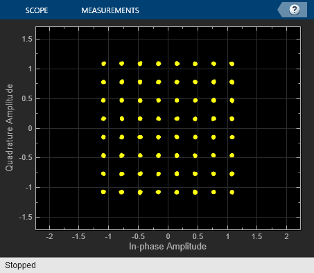
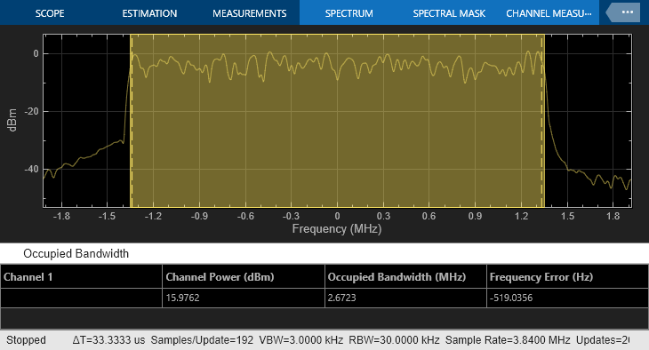
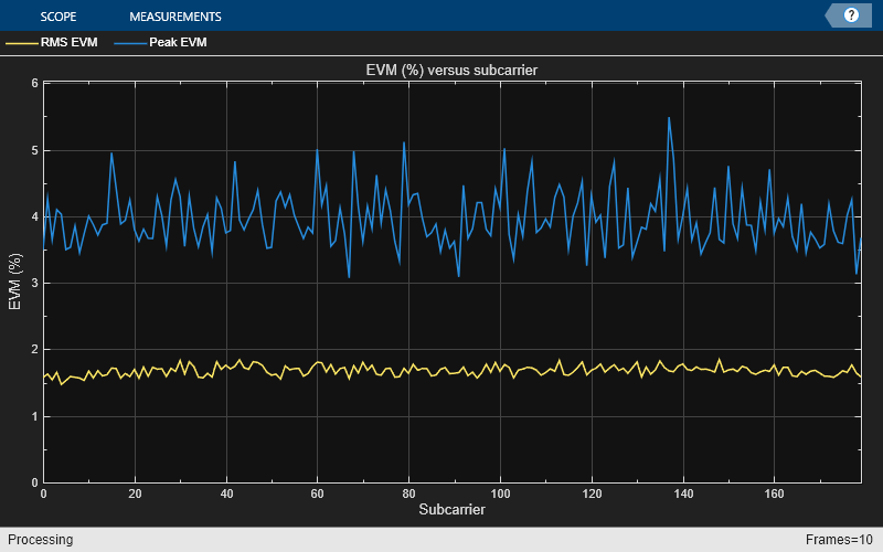
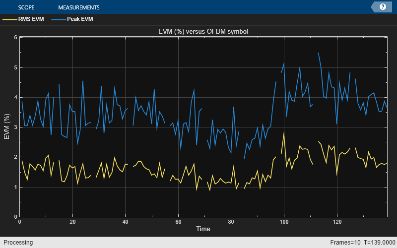
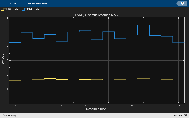
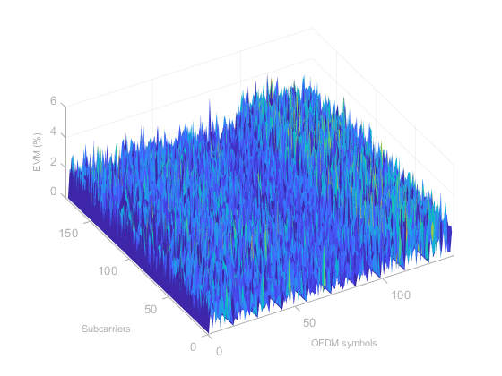
According to TS 36.104, the maximum EVM when the constellation is 64-QAM is 8%. As the overall EVM is around 1.7%, this architecture falls within the requirements of TS 36.104.
Nonlinear HPA (IBO = 6 dB). To operate at an IBO level of 6 dB, set the Available power gain parameter of the VGA block to 6 dB.
set_param([modelName '/RF Transmitter'],'vgaGain','6');
sim(modelName);
slmsgviewer.DeleteInstance();

% Restore to default parameters
set_param([modelName '/RF Transmitter'],'vgaGain','0');
Low edge EVM, subframe 0: 2.946%
High edge EVM, subframe 0: 2.970%
Low edge EVM, subframe 1: 2.687%
High edge EVM, subframe 1: 2.703%
Low edge EVM, subframe 2: 2.689%
High edge EVM, subframe 2: 2.708%
Low edge EVM, subframe 3: 2.673%
High edge EVM, subframe 3: 2.693%
Low edge EVM, subframe 4: 2.601%
High edge EVM, subframe 4: 2.606%
Low edge EVM, subframe 5: 2.354%
High edge EVM, subframe 5: 2.371%
Low edge EVM, subframe 6: 2.568%
High edge EVM, subframe 6: 2.588%
Low edge EVM, subframe 7: 3.653%
High edge EVM, subframe 7: 3.651%
Low edge EVM, subframe 8: 3.634%
High edge EVM, subframe 8: 3.631%
Low edge EVM, subframe 9: 3.201%
High edge EVM, subframe 9: 3.202%
Averaged low edge EVM, frame 0: 2.935%
Averaged high edge EVM, frame 0: 2.945%
Averaged EVM frame 0: 2.945%
Averaged overall EVM: 2.945%
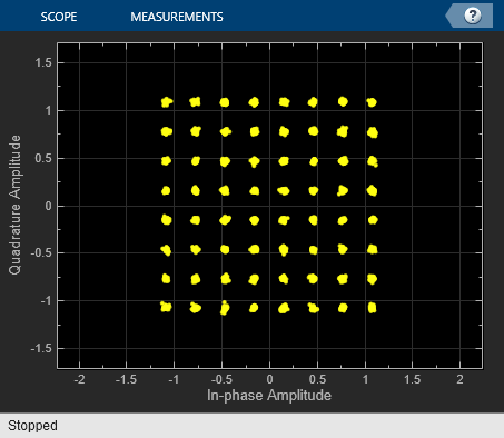
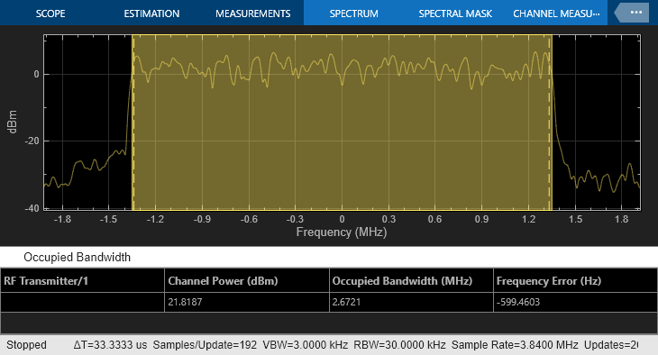
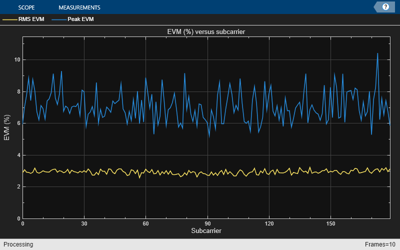
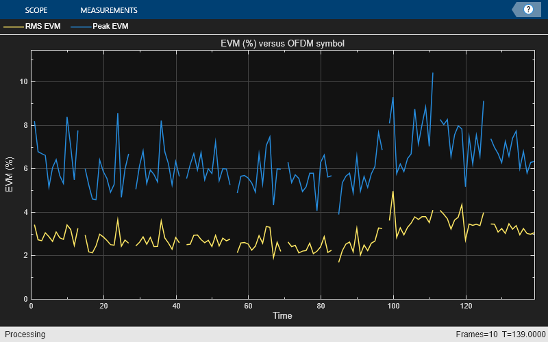
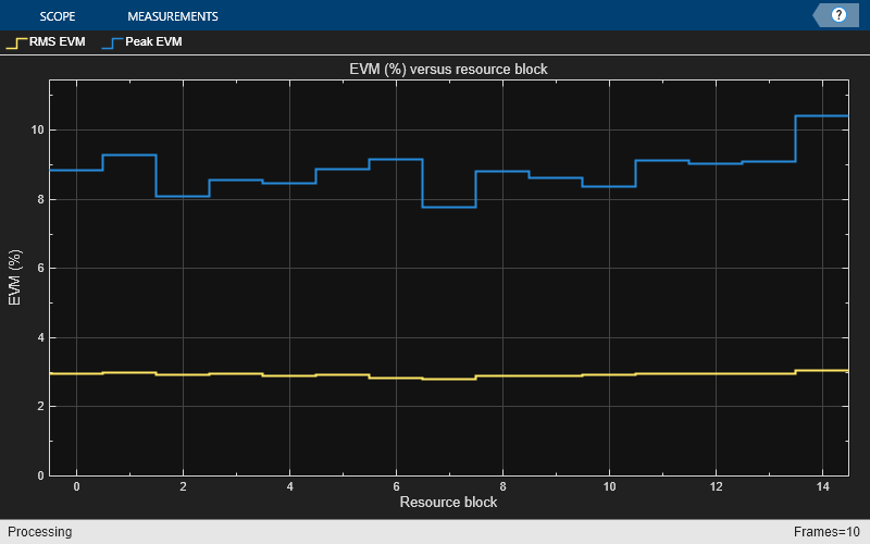


Compared to the previous case, the constellation diagram is more distorted. In terms of measurements, the overall EVM, around 3%, still falls within the requirements of TS 36.104.
If you want to push the HPA to operate further in the nonlinear region, you will need to oversample the signal (around 5 times its baseband bandwidth) so that the simulation bandwidth is large enough to capture in-band spectral regrowth.
Summary and Further Exploration
This example demonstrates how to model and test an LTE RF transmitter in Simulink. The RF transmitter consists of an IQ modulator, a bandpass filter and amplifiers. To evaluate the performance, the Simulink model considers EVM measurements. The example highlights the effect of HPA nonlinearities on the performance of the RF transmitter. You can explore the impact of altering other impairments as well. For example:
Increase I/Q imbalance by using the I/Q gain mismatch (dB) and I/Q phase mismatch (Deg) parameters on the IQ Modulator tab of the RF Transmitter Subsystem block.
Increase the phase noise by using Phase noise offset (Hz) and Phase noise level (dBc/Hz) parameters on the IQ Modulator tab of the RF Transmitter Subsystem block.
The RF Transmitter Subsystem block is configured to work with the current E-TM waveform parameters selected in the LTE Test Model block and with the LTE carrier centered at 2140 MHz. This carrier is within the E-UTRA operating band 1. If you modify the Center frequency (MHz) parameter of the RF Transmitter Subsystem block or the waveform configuration of the LTE Test Model block, check if you need to update the parameters of the RF Transmitter components as these parameters are set to work with the current example configuration. For instance, a change in the carrier frequency requires revising the Passband frequencies and Stopband frequencies parameters of the Bandpass Filter block inside the RF transmitter. If you select a bandwidth wider than 3 MHz, check if you need to update the Impulse response duration and Phase noise frequency offset (Hz) parameters of the IQ Modulator (RF Blockset) block. The phase noise offset determines the lower limit of the impulse response duration. If the phase noise frequency offset resolution is high for a given impulse response duration, a warning message appears, specifying the minimum duration suitable for the required resolution.
You can use this example as the basis for testing E-TM waveforms for different RF configurations. You can try replacing the RF Transmitter Subsystem block by another RF subsystem and then configure the model accordingly.
References
3GPP TS 36.141 "E-UTRA; Base Station (BS) conformance testing" 3rd Generation Partnership Project; Technical Specification Group Radio Access Network.
3GPP TS 36.104 "E-UTRA; Base Station (BS) radio transmission and reception" 3rd Generation Partnership Project; Technical Specification Group Radio Access Network.
3GPP TS 36.101. "E-UTRA; User Equipment (UE) radio transmission and reception." 3rd Generation Partnership Project; Technical Specification Group Radio Access Network.