getpads
Description
Examples
getpads of Single Ended Via
This example shows how to use the getpads function of a single ended via to generate a pad stack
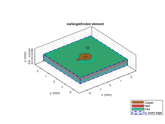
via = viaSingleEnded
via =
  viaSingleEnded with properties:

   Conducting Layers
                        SignalLayer: [1 7]
                        GroundLayer: [3 5 9]
                          Conductor: [1x1 metal]

   Dielectric Layers
                          Substrate: [1x1 dielectric]

   Signal Vias
                 SignalViaLocations: [0 0 1 7]
                  SignalViaDiameter: 2.5000e-04
          SignalViaFinishedDiameter: 2.0000e-04
                       SignalViaPad: [1x1 antenna.Circle]
                   RemoveUnusedPads: 1
                   SignalViaAntipad: [1x1 antenna.Circle]

   Ground Return Vias
           GroundReturnViaLocations: [1.0000e-03 1.0000e-03 1 9]
            GroundReturnViaDiameter: 2.5000e-04
    GroundReturnViaFinishedDiameter: 2.0000e-04

   Ports
                        SignalTable: {2x4 cell}
SPad = getpads(via)
SPad=1×5 cell array
    {1x1 antenna.Circle}    {0x0 double}    {0x0 double}    {1x1 antenna.Circle}    {0x0 double}
show(via)
Input Arguments
Output Arguments
Version History
Introduced in R2024a
You can also select a web site from the following list:
Americas
- América Latina (Español)
- Canada (English)
- United States (English)
Europe
- Belgium (English)
- Denmark (English)
- Deutschland (Deutsch)
- España (Español)
- Finland (English)
- France (Français)
- Ireland (English)
- Italia (Italiano)
- Luxembourg (English)
- Netherlands (English)
- Norway (English)
- Österreich (Deutsch)
- Portugal (English)
- Sweden (English)
- Switzerland
- United Kingdom (English)