slice
Description
Examples
Create pcbComponent object from rfpcb catalog object - in this example a coupled microstripline filter catalog object is used. Note that solver type must be specified MoM for slice function and 2-D solver to function.
cfilter = pcbComponent(coupledMicrostripLine(Conductor=metal('copper')))cfilter =
pcbComponent with properties:
Name: 'Coupled Line Filter'
Revision: 'v1.0'
BoardShape: [1×1 antenna.Rectangle]
BoardThickness: 0.0016
Layers: {[1×1 antenna.Polygon] [1×1 dielectric] [1×1 antenna.Rectangle]}
FeedFormat: 'FeedLocations'
FeedLocations: [4×4 double]
FeedDiameter: 0.0026
ViaLocations: []
ViaDiameter: []
FeedViaModel: 'strip'
Conductor: [1×1 metal]
Tilt: 0
TiltAxis: [0 0 1]
Load: [1×1 lumpedElement]
SolverType: 'MoM'
IsShielded: 0
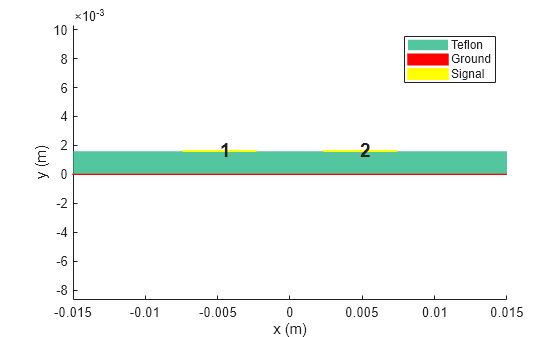
Use slice function on pcbComponent to create pcb2D object. Visualize object, which has two signal traces in this case. All signal traces must be specified within a single cell. Note that the 2-D field solver's coordinate axes convention differs from the convention used for 3-D PCB structures: The y-axis runs in a vertical direction through layers of the 2D structure, with y=0 corresponding to the bottom of the PCB structure; the x-axis runs perpendicular to the y-axis and direction of signal propagation.
pcb2d = slice(cfilter)
pcb2d =
  pcb2D with properties:

           Name: 'MyPCB2D'
     BoardWidth: 0.0300
    BoardCenter: 0
         Layers: {[1×2 trace2D]  [1×1 dielectric]  [1×1 trace2D]}
show(pcb2d)
Calculate s parameters and RLGC properties at 1.9 GHz.
spar = sparameters(pcb2d,1.9e9)
spar =
  sparameters with properties:

      Impedance: 50
       NumPorts: 4
     Parameters: [4×4 double]
    Frequencies: 1.9000e+09
spar.Parameters
ans = 4×4 complex

   0.0042 + 0.0203i   0.0255 - 0.0041i  -0.6235 + 0.1163i   0.1353 + 0.7190i
   0.0255 - 0.0041i   0.0042 + 0.0203i   0.1353 + 0.7190i  -0.6235 + 0.1164i
  -0.6235 + 0.1163i   0.1353 + 0.7190i   0.0042 + 0.0203i   0.0255 - 0.0041i
   0.1353 + 0.7190i  -0.6235 + 0.1164i   0.0255 - 0.0041i   0.0042 + 0.0203i
pcb2Dproperties = rlgc(pcb2d,1.9e9);
R2D = pcb2Dproperties.R
R2D = 2×2

    2.6930    0.1773
    0.1773    2.6930
L2D = pcb2Dproperties.L
L2D = 2×2
10-6 ×

    0.2234    0.0141
    0.0141    0.2234
G2D = pcb2Dproperties.G
G2D = 2×2
10-3 ×

    0.1824    0.0008
    0.0008    0.1824
C2D = pcb2Dproperties.C
C2D = 2×2
10-10 ×

    0.9041   -0.0281
   -0.0281    0.9041
Input Arguments
Name-Value Arguments
Output Arguments
Version History
Introduced in R2026a