Pre-Layout Analysis of Serial Link Projects
Analyze serial link projects before designing board layouts
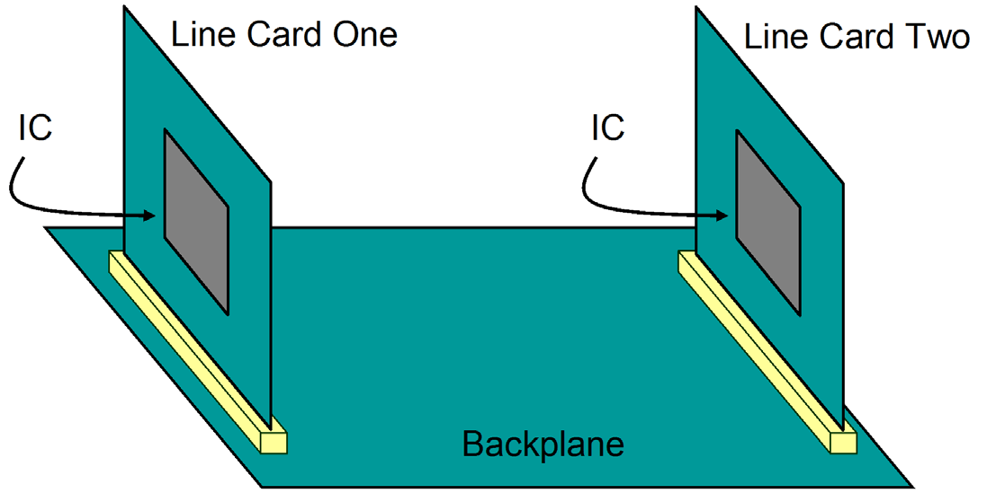
You can run simulations using IBIS-AMI models to determine the system-level noise before designing PCB layouts. The pre-layout analysis environment helps you to generate design guidelines for your board layouts, package layouts, connectors, and cabling.
Apps
| Serial Link Designer | Analyze PCB designs for serial link applications (Since R2021b) |
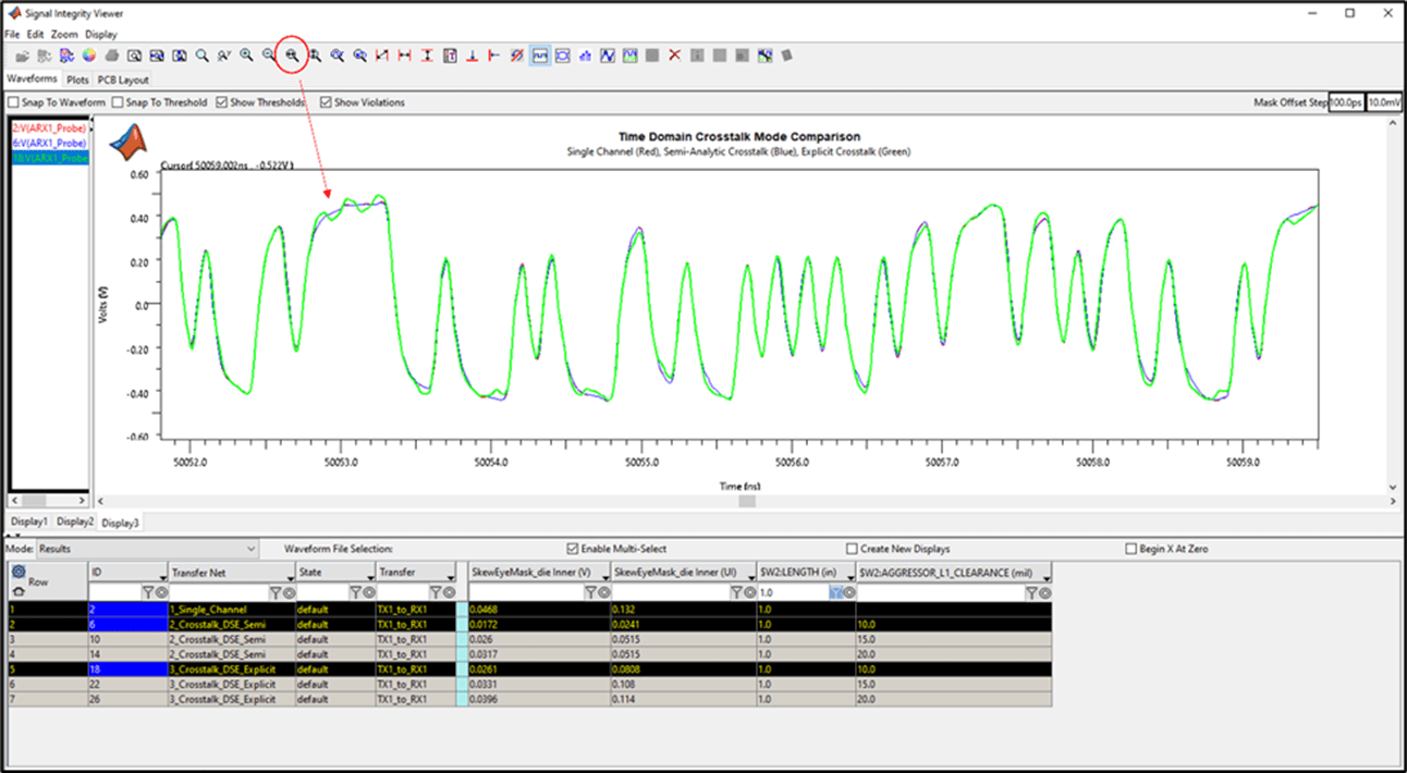
| Signal Integrity Viewer | View the signal integrity results of Serial Link Designer or Parallel Link Designer apps (Since R2021b) |
Objects
si.MER | Reconstruct MER waveform and estimate MER statistical eye of nonlinear systems (Since R2024b) |
Topics
- Pre-Layout Analysis of Serial Link
Learn the basics of pre-layout analysis.
- Customize Serial Link Project for Pre-Layout Analysis
Edit transmission line models, designators, S-parameters, and IBIS files to customize pre-layout analysis.
- Results of Pre-Layout Analysis in Serial Link
View, interpret, and debug the pre-layout analysis results.

