Refine RF Receiver Model and Simulate RF Impairments
This example shows how to refine the RF receiver with the desired noise figure NF = 10.7 dB and gain G = 51.5 dB specifications determined in the Determine RF Receiver Specifications example. The RF receiver is implemented using four discrete subcomponents with these characteristics:
SAW Filter: Noise Figure = 2.3 dB, Gain = – 3 dB
LNA: Noise Figure = 7 dB, Gain = 22 dB
Passive Mixer or Demodulator: Noise Figure = 10 dB, Gain = – 7 dB
VGA: Noise Figure = 14 dB, Gain = 37 dB
The gain and noise figure budget can be verified using the RF Budget Analyzer app. In the app:
Use Friis equations or Harmonic Balance analysis to determine the noise, gain, and nonlinearity budget of an RF chain, also taking into account impedance mismatches.
Explore the receiver design space and determine how to break down the specifications across the elements of the chain.
Determine which element has the largest contribution to the noise and nonlinearity budget.
Generate an RF receiver model with which you can perform multi-carrier simulation and further modify.
Type rfBudgetAnalyzer('TopDownRFReceiverDesign.mat') at the command line to visualize the RF receiver in the RF Budget Analyzer app.

The signal input frequency, power, and bandwidth has been set consistently with the system specifications. The center frequency of the signal is assumed to be at 2.45 GHz, typical of the ZigBee standard. The SAW filter performance is derived from a Touchstone file that specifies S-parameter characteristics. Typically, an LNA with low noise and high gain follows the SAW filter, which greatly reduces the impact of the noise figure of the components after the LNA. As the SAW filter S-parameters are frequency dependent, NF and Gain for the SAW filter have been computed at 2.45 GHz.
The demodulator LO frequency has been set equal to the RF center frequency, indicating a direct conversion implementation based on a quadrature mixer. As the gain of quadrature architectures is measured with respect to either the I or the Q branch, the overall gain budget has been reduced by 3 dB. The overall receiver gain, when combining the I and Q branches into a complex signal, is approximately 52 dB and marginally more favorable than the given budget of 51.5 dB. The budget analysis also confirms that the SNR matches the expected value.
You can manually build the circuit envelope model of the RF receiver by using blocks from the Circuit Envelope library, or it can be automatically generated using the RF Budget Analyzer app.
Create a Circuit Envelope Model of RF Receiver
Using the circuit envelope modeling approach, implement the receiver with a direct conversion architecture and continue refining the RF receiver performance by adding realistic RF impairments.
The circuit envelope model of the RF receiver allows to:
Verify that the RF receiver implementation is correct while also modeling the impact of imperfections such as non-linearity, I/Q imbalance, LO leakage, phase noise and colored noise.
Use the measured S-parameters data and specify broadband impedances (50 ohm) to explicitly model the power transfer between blocks including impedance mismatches
Evaluate the impact of out-of-band interfering signals using multi-carrier simulation, and design digital signal processing correction algorithms
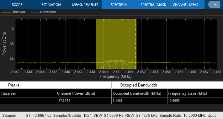
Comparing the spectra, power measurements, and ChER to the link-level model from Develop ZigBee-Like Baseband Transmitter and Receiver there are no significant performance differences. The marginal improvement is due to the higher gain of the circuit envelope chain (52 dB) compared to the original gain of the reference receiver (51.5 dB).
Notice that this model is simulated over a four times larger simulation bandwidth equal to 16 MHz. A larger simulation bandwidth is required when simulating non-linear and frequency dependent broadband effects. The reference receiver has been added to the model to make easier the comparison as we add RF impairments to the receiver.
At 2.45 GHz (center frequency of the input signal) the SAW filter introduces a phase rotation of approximately 58 degrees that must be compensated. In general, a synchronization mechanism is required in baseband receivers to recover the constellation. In this model, a fixed phase rotation equal and opposite to the one introduced by SAW filter has been introduced in the baseband receiver.
model = 'RxCE';
open_system(model);
ws = warning('off','simrf:simrfV2errors:DerivedNoiseNotPassive');
sim(model);
warning(ws)


Use Circuit Envelope Model to Simulate RF Impairments
The simulation of the circuit envelope model does not include any RF imperfection beyond thermal noise. The variables listed below are set in the MATLAB workspace and allow you to include LO isolation, even order nonlinearity, and phase noise in the demodulator, as well as the antenna impedance.
loPhaseNoise = – 200; (dBm/Hz)
loPhaseNoiseFreq = 2e5; (Hz)
antennaImpedance = 50; (Ohm)
demodIP2 = inf; (dBm)
loToRFIsolation = inf; (dB)
Run the simulation with increased phase noise. As the thermal noise floor is already relatively high, the impact on the ChER is less than 1%.
loPhaseNoise = [-70 -80 -95 -110 -120]; % dBm/Hz
loPhaseNoiseFreq = [0.2 1 2 3 7]*1e6;   % Hz
open_system(model);

ws = warning('off','simrf:simrfV2errors:DerivedNoiseNotPassive');
sim(model);

Run the simulation with an antenna impedance of 75 ohms, typical of a dipole without a matching network. Even a relatively modest impedance mismatch reduces the gain at the beginning of the chain with a significant impact on the noise budget. As a result of the antenna mismatch, the ChER is degraded by almost 2%.
antennaImpedance = 75; %Ohm
open_system(model);

ws = warning('off','simrf:simrfV2errors:DerivedNoiseNotPassive');
sim(model);

Run the simulation with finite IP2. As the amplitude of the input signal is small, this has no impact on the ChER. Even at full scale, with input power equal to – 50 dBm, the effects of finite IP2 remains negligible.
demodIP2 = 55;  % dBm
open_system(model);

ws = warning('off','simrf:simrfV2errors:DerivedNoiseNotPassive');
sim(model);

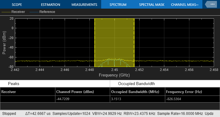
Run the simulation with finite, but very low, LO isolation. The reciprocal mixing of the LO signal causes a DC offset of – 40 dBm that can be measured with the Spectrum Analyzer. Because of the DC offset, the ChER is degraded. Either a demodulator with higher isolation (>100 dB) or a DC offset compensation algorithm is required to meet the specifications.
loToRFIsolation = 90; %dB
open_system(model);
ws = warning('off','simrf:simrfV2errors:DerivedNoiseNotPassive');
sim(model);
