Diode
R2026bPiecewise linear, exponential, or tabulated diode
Diode block

To add a block to a model, double-click the canvas and start typing the block name. Then, select the block from the list.
Libraries:
Simscape /
Electrical /
Semiconductors & Converters
Description
The Diode block models a diode with a piecewise linear, tabulated, or exponential relationship between current I and voltage V:
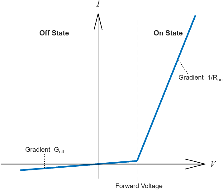
Piecewise linear — Specify the forward voltage, on resistance, and off conductance. The I-V curve consists of two linear regions separated by a forward voltage threshold: a high-resistance off state and a low-resistance on state.
Tabulated I-V curve — Specify tabular data for forward current as a function of junction temperature and forward voltage. The software interpolates between measured data points, with linear extrapolation beyond the tabulated range.
Exponential — Use the Shockley diode equation to model the exponential relationship between diode voltage and current. The saturation current varies with temperature based on the semiconductor energy gap.
Choose the diode model based on the level of fidelity that you need to meet your design goals and the data that you have available to parameterize the block. You manage the level of fidelity by setting the Modeling option parameter to one of these options:
Ideal— Use a piecewise linear I-V curve. The block has no thermal port. This simple model simulates quickly and does not include reverse recovery losses or charge dynamics.Ideal with thermal losses— Choose a piecewise linear or tabulated I-V curve. The block models the reverse recovery losses as an energy loss at switching events and does not model charge dynamics. The block has an exposed thermal port.Detailed with charge dynamics— Choose a tabulated or exponential I-V curve. The block models the charge dynamics. You can specify a fixed capacitance or a depletion-mode capacitance. You can also model charge reverse recovery using the Lauritzen charge model. The charge-dynamics model captures reverse recovery losses implicitly through continuous electrical power dissipation. The block has an optional thermal port. This model provides the highest fidelity for analyzing transient effects and loss distribution.
For more information about choosing the level of fidelity that you need to meet your design goals, see Choose Blocks to Model Semiconductor Devices.
Note
Before R2026b: The Modeling option parameter determines only whether you expose the thermal port. As a result of this change, the Diode block parameters, dependencies, and variables have changed. If you are using a previous release or working with models that you developed in a previous release, see Manage model fidelity using a simpler block mask for more information.
When you set the Modeling option parameter to
Ideal, the Diode block is similar to
the simpler Diode block in the Simscape™ Foundation Library. Use the Diode block in the
Simscape
Electrical™ library, when you want to:
Model multiple diodes in series or parallel using a single Diode block.
Model Zener diodes.
Model faults.
Plot block-level characteristics using buttons in the Utilities settings.
This table summarizes the features that each level of fidelity supports, with links to the relevant section in the documentation.
| Modeling option | |||
|---|---|---|---|
| Ideal | Ideal with thermal losses | Detailed with charge dynamics | |
| Diode model (I-V parameterization) | |||
Zener diodes For more information, see Model Zener diode. | Supported | Supported | Supported |
| Reverse recovery losses | Not modeled | Modeled explicitly as an energy loss at switching events For more information, see Reverse Recovery Losses. | Included implicitly in the continuous electrical power dissipation resulting from the charge-dynamics equations |
| Junction capacitance | Not modeled | Not modeled | Modeled For more information, see Junction Capacitance. |
| Charge dynamics | Not modeled | Not modeled | Modeled For more information, see Charge dynamics. |
Temperature dependence on I-V characteristics For more information, see Temperature Dependence. | Not modeled |
|
|
Effects of electrical losses on device temperature For more information, see Modeling Thermal Effects. | Not modeled The block converts conduction losses to heat that is external to the system. | Modeled The block converts electrical losses to heat by stepping up the junction temperature at the thermal port. | Optional If you do not enable the thermal port, the blocks converts electrical losses to heat that is external to the system. If you enable the thermal port, the block converts electrical losses to heat by stepping up the junction temperature at the thermal port. |
Initial targets and nominal values For more information, see Variables. | Supported | Supported | Supported |
Parameterization tools For more information, see Parameterization. | Supports predefined parameterizations |
|
|
Faults For more information, see Faults. | Supported | Supported | Supported |
Basic characteristics and derived data sheets For more information, see Utilities. | Supported | Supported | Supported |
Piecewise Linear Diode
To model a piecewise linear diode, choose one of these options:
Set the Modeling option parameter to
Ideal.Set the Modeling option parameter to
Ideal with
        thermal losses
and set the Diode model parameter toPiecewise linear.
When the diode voltage exceeds the value of the Forward voltage parameter, the diode is forward biased and in the on state. In this region, the current increases with voltage at a gradient of 1/Ron, where Ron is the value of the On resistance parameter. Otherwise, the diode is in the off state and behaves like a linear resistor with a small conductance equal to the Off conductance parameter value, Goff. This figure shows a typical I-V curve with an exaggerated value of Goff.
If you select the Model Zener diode parameter, the I-V curve includes a third conduction region for reverse breakdown at voltages less than -BV where BV is the breakdown voltage. In this region, the current increases with increasing voltage at a gradient of 1/Rz where Rz is the Zener resistance.
Tabulated Diode
To model a diode with a tabulated I-V curve:
Set the Modeling option parameter to
Ideal with thermal lossesorDetailed with charge dynamics.Set the Diode model parameter to
Tabulated I-V curve.
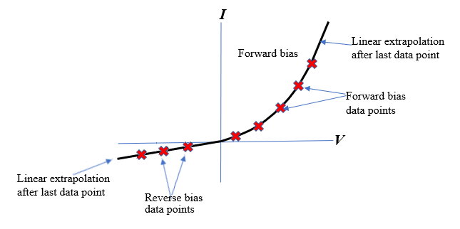
This figure shows the implementation of the tabulated diode option:
If you select the Model Zener Diode parameter, you can also model the tabulated reverse I-V characteristics. If you do not select the Model Zener Diode parameter, the block models the reverse characteristics by using the Off conductance parameter:
If the voltage is less than -1 V, the block models the I-V relationship with a constant off-state conductance equal to the value of the Off conductance parameter. The value you specify must be less than the gradient of the forward I-V curve for small positive voltages.
If the voltage is between -1 V and 0 V, the block uses
makimainterpolation so that the I-V curves for forward and reverse bias overlap smoothly.
The block uses makima interpolation to find intermediate values. If the voltage or current exceed the tabulated data range, the block uses linear extrapolation after the last I-V data point.
Exponential Diode
To model an exponential diode, set the Modeling option parameter to
Detailed with charge dynamics and set the Diode
model parameter to Exponential.
The exponential diode model uses this relationship between the diode current and the diode voltage,
where:
q is the elementary charge on an electron (1.602176e-19 C).
k is the Boltzmann constant (1.3806503e-23 J/K).
BV is the reverse breakdown voltage.
N is the emission coefficient.
IS is the saturation current.
Tm1 is the Measurement temperature parameter value. This parameter defines the operating temperature at which the electrical properties of the modeled device are equal to the corresponding block parameters values.
When (qV / NkTm1) > 80, the block replaces with (qV / NkTm1 – 79)e80, which matches the gradient of the diode current at (qV / NkTm1) = 80 and extrapolates linearly. When (qV / NkTm1) < –79, the block replaces with (qV / NkTm1 + 80)e–79, which also matches the gradient and extrapolates linearly. Typical electrical circuits do not reach these extreme values. The block provides this linear extrapolation to improve convergence when solving for the constraints during simulation.
If you select the Model Zener Diode parameter, the block uses the
finite value of BV that you specify to model the sharp increase in reverse
current as the voltage approaches -BV. If you clear this parameter, the block
sets BV = inf, so the equation for V >
-BV always applies.
The reverse breakdown voltage and saturation current are functions of temperature. You specify the reverse breakdown voltage at the measurement temperature using the Reverse breakdown voltage parameter. How the block calculates the saturation current at the measurement temperature depends on which option you select for the Parameterization parameter in the Main settings.
When you set Parameterization to Use parameters IS and
N, you specify the saturation current and emission coefficient using the
Saturation current IS and Emission coefficient N
parameters.
When you set Parameterization to Use two I-V curve data
points, you specify two voltage and current measurement points on the diode I-V
curve and the block derives the IS and N values using
these equations,
where:
Vt = kTm1 / q.
V1 and V2 are the values in the Voltages [V1 V2] vector.
I1 and I2 are the values in the Currents [I1 I2] vector.
When you set Parameterization to Use an I-V data point
and IS, the block calculates N using this equation.
When you set Parameterization to Use an I-V data point
and N, the block calculates IS using this equation.
If you model temperature dependence, the block modifies BV and IS to account for differences between the measurement temperature and the simulation temperature. For more information, see Temperature Dependence.
Zener Diode
When a diode is sufficiently reverse biased, it enters reverse breakdown and begins to conduct in the reverse direction. To model this behavior, select the Model Zener diode parameter and specify a finite value for the Reverse breakdown voltage parameter. All three values of the Modeling option parameter support Zener diode modeling.
How the block models reverse breakdown depends on the diode I-V model:
Piecewise linear — The I-V curve gains a third conduction region below -BV, where current increases with a gradient of 1/Rz. You specify the breakdown voltage and Zener resistance.
Tabulated I-V curve — You specify the reverse I-V characteristics directly as tabulated data. This replaces the constant off-conductance you need to provide if you clear the Model Zener diode parameter. For more information, see Tabulated Diode.
Exponential — The reverse breakdown voltage BV is part of the Shockley diode equation. The block models the sharp increase in reverse current as the voltage approaches -BV. For more information, see Exponential Diode.
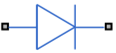
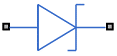
The Diode block icon updates automatically depending on whether you model a Zener diode and whether you expose the thermal port.
| Thermal Port | Model a Zener diode Parameter Value | Block Icon |
|---|---|---|
| Not exposed | Off |
|
On |
| |
| Exposed | Off |
|
On |
|
Reverse Recovery Losses
Reverse recovery loss is one of the main sources of thermal loss in diodes. When the diode turns off, current briefly continues flowing in reverse as stored charge in the junction depletes. The diode dissipates this energy every time it turns off, transitioning from its conducting state to the open-circuit state.
To model reverse recovery losses explicitly, without modeling charge dynamics, set the
Modeling option parameter to Ideal with thermal
losses. The block represents the losses that the charge creates during reverse
recovery as an instantaneous loss. Alternatively, if you set the Modeling
option parameter to Detailed with charge dynamics, the
block models reverse recovery losses through continuous charge dynamics rather than
instantaneous energy events. This option also supports junction capacitance modeling. For more
information, see Junction Capacitance and
Charge Dynamics.
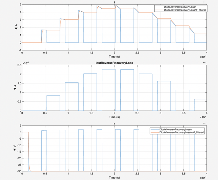
This figure shows the current, reverse recovery energy, and voltage of the diode in a switching regime inside a half-bridge. The middle plot shows the energy dissipated at each turn-off event.
The block applies reverse recovery losses by stepping up the junction temperature with a value equal to the reverse recovery loss divided by the total thermal mass at the junction.
If you set the Reverse recovery loss model parameter to
Fixed loss, the value of the Reverse recovery
loss parameter specifies the energy dissipated during each turn-off event. If you
select the Scale reverse recovery loss with current and voltage parameter,
then the block scales this loss value linearly by the on-state current and the off-state
voltage. To use scaling values that are close to the instantaneous values, set the
Filter time constant for voltage and current values parameter to a value
that is lower than the fastest switching period.
If you set the Reverse recovery loss model parameter to
Tabulate loss with Tj and If or Tabulate loss with Tj,
If, and Vrec, the block uses a lookup table to determine the dissipated energy as
a function of the junction temperature and the forward current just before the switching event.
The three-dimensional option also tabulates by turn-off voltage, whereas the two-dimensional
option linearly scales the losses by the off-state voltage relative to the Turn-off
voltage when measuring recovery loss, Vrec parameter value. Both options use delayed
values for the current and voltage. To use a value in the lookup table that is close to the
instantaneous value, set the Filter time constant for voltage and current
values parameter to a value that is lower than the fastest switching
period.
Note
The lastReverseRecoveryLoss variable in the logged simulation data
includes the reverse recovery losses as a pulse with an amplitude equal to the energy loss. If
you use a script to sum the total losses over a defined simulation period, you must sum the
pulse values at each pulse rising edge. Alternatively, you can extract conduction and switching
losses from logged data using the ee_getPowerLossSummary and ee_getPowerLossTimeSeries functions. To learn how to log and plot simulation data,
see the Log and Plot Simulation Data example.
The power_dissipated variable in the logged simulation data does not
include switching losses because the block models the losses as instantaneous events. The
power_dissipated variable reports ohmic on-state losses.
Junction Capacitance
The depletion region of a diode acts as a voltage-dependent capacitance that affects
transient switching behavior. To model the junction capacitance, set the Modeling
option parameter to Detailed with charge dynamics. This
depletion-layer capacitance is distinct from the diffusion charge due to injected minority
carriers, and both effects can be active at the same time. For more information about diffusion
charge modeling, see Charge
Dynamics.
You choose how to parameterize the junction capacitance by using the
Parameterization parameter in the Capacitance
settings. The Include fixed or zero junction capacitance option uses
a constant capacitance value. The Use C-V curve data points and
Use parameters CJO, VJ, M & FC options use a nonlinear SPICE
depletion capacitance model to calculate a junction capacitance that depends on the junction
voltage. The options differ only in how you supply the coefficients. Both options use the
forward-bias capacitance coefficient FC. This table shows which other
coefficients you need to provide and when to choose each option.
| Parameterization Option | Description | Use Case |
|---|---|---|
Include fixed or zero junction capacitance | The capacitance is fixed at the value you specify. Set the value to zero to disable capacitance modeling. | Capacitance is not critical or you only have a single-value estimate. |
Use C-V curve data points | You specify three data points of the reverse voltage and the corresponding capacitance. The block estimates SPICE coefficients CJO, VJ, and M internally. | You have data sheet C-V curve values. |
Use parameters CJO, VJ, M & FC | You specify the SPICE junction capacitance parameters CJO, VJ, and M directly. | You have SPICE parameters from a .model card or IBIS file. |
When you set the Parameterization parameter to Use C-V
curve data points, the block calculates CJO,
VJ, and M using these equations,
where:
VR1, VR2, and VR3 are the values in the Reverse bias voltages [VR1 VR2 VR3] vector.
C1, C2, and C3 are the values in the Corresponding capacitances [C1 C2 C3] vector.
The reverse bias voltages (defined as positive values) must satisfy VR3 > VR2 > VR1. This means that the capacitances must satisfy C1 > C2 > C3 as reverse bias widens the depletion region and hence reduces capacitance. Violating these inequalities results in an error. Voltages VR2 and VR3 should be well away from the junction potential VJ. Voltage VR1 should be less than the junction potential VJ, with a typical value for VR1 being 0.1 V.
For both the Use C-V curve data points and Use
parameters CJO, VJ, M & FC options, the block defines the voltage-dependent
junction capacitance in terms of the charge of junction capacitance
Qj as:
For V < FC·VJ:
For V ≥ FC·VJ:
where:
V is the junction capacitance voltage.
These equations are the same as used in [2], except the block does not model the temperature dependence of VJ and FC.
Charge Dynamics
For applications such as commutation diodes, modeling diode charge dynamics is important. When a forward-biased diode has a reverse voltage applied across it, it takes time for the charge to dissipate and hence for the diode to turn off. The time taken for the diode to turn off is captured primarily by the transit time parameter. Once the diode is off, any remaining charge dissipates at a rate determined by the carrier lifetime.
This diffusion charge model is separate from the depletion-layer junction capacitance, which you can configure independently. For more information about junction capacitance modeling, see Junction Capacitance.
To model the charge dynamics, set the Modeling option parameter to
Detailed with charge dynamics. If you only need to account for
reverse recovery energy losses without modeling the underlying charge physics, set the
Modeling option parameter to Ideal with thermal
losses instead. For more information, see Reverse Recovery
Losses.
The Diode block uses the model of Lauritzen and Ma [3] to capture these effects. These are the defining equations.
| (1) |
| (2) |
| (3) |
i is the diode current.
qE is the junction charge.
qM is the total stored charge.
TM is the transit time.
τ is the carrier lifetime.
vD is the voltage across the diode.
vF is the diode forward voltage.
R is the diode on resistance.
G is the diode off conductance.
This graphic shows a typical reverse-mode current characteristic for a diode device.
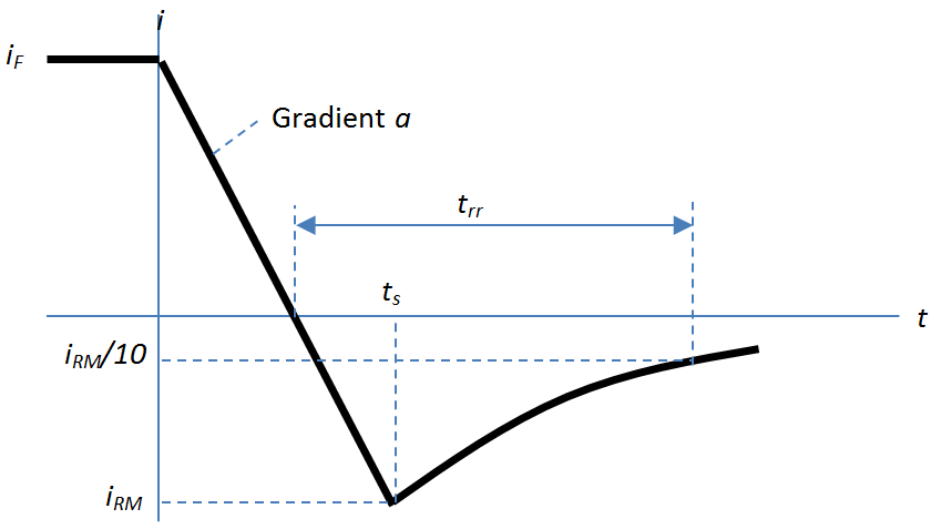
where:
iRM is the peak reverse current.
iF is the starting forward current when measuring iRM.
a is the rate of change of current when measuring iRM.
trr is the reverse recovery time.
Data sheets for diodes quote values for peak reverse current for an initial forward current and a steady rate of change of current. The data sheet might also provide values for reverse recovery time and total recovery charge.
The block calculates transit time TM and carrier lifetime τ based on the values you enter for the Charge Dynamics parameters. The block uses TM and τ to solve the charge dynamics equations 1, 2, and 3.
During initial current drop in reverse mode, the diode is still on, and the rate of change of current is determined by an external test circuit.
First, the block uses equation 1 to perform this calculation.
| (4) |
Then, it substitutes equation 4 into equation 2.
| (5) |
Then, it solves equation 5 for qM,
| (6) |
When t is zero, i = iF and qM = τiF because the system is in steady state.
Substituting these relationships into equation 6 and solving the equation gives k = aτ2.
Therefore,
| (7) |
The block substitutes these values into equation 1.
| (8) |
| (9) |
Then, the block expresses time ts in terms of iRM, iF, and a.
| (10) |
Consider the diode recovery, that is, when t > ts. The diode is reverse biased, and current and junction charge are effectively zero.
The current is defined by this equation.
| (11) |
where:
| (12) |
The block now relates the expression in equation 12 to the reverse recovery time trr.
When the current is
Therefore,
| (13) |
| (14) |
The block uses equations 9 and 14 to calculate values for TM and τ. The calculation uses an iterative scheme because of the exponential term in equation 9.
In addition to allowing you to specify reverse recovery time trr directly, the block supports three alternative parameterizations. The block can derive trr from either of these parameters:
Reverse recovery time stretch factor λ
Reverse recovery charge Qrr, when the data sheet specifies this value instead of the reverse recovery time.
Reverse recovery energy Erec, when the data sheet specifies this value instead of the reverse recovery time.
The relationship between reverse recovery time stretch factor λ and trr is expressed by the equation
Reverse recovery time must be greater than and a typical value is
Therefore, a typical value for λ is 3. λ must be greater than 1.
Reverse recovery charge Qrr is the integral over time of the reverse current from the point where the current goes negative until it decays back to zero.
The initial charge, to time ts (as shown in the figure), is expressed by this equation:
| (15) |
Integrating equation 11 gives the charge between times ts and inf. This charge is equal to
Therefore, total reverse recovery charge is given by this equation:
| (16) |
Rearranging equation 16 to solve for τrr and substituting the result into equation 14 gives an equation that expresses trr in terms of Qrr:
Alternatively, the block calculates τrr by using the reverse recovery energy, Erec. This equation defines the diode voltage curve:
| (17) |
If , which is a common condition for the reverse recovery test circuit, the block calculates the maximum diode reverse voltage as:
Because the drop time value is small, the block assumes that the diode current drop is linear:
| (18) |
Then, it substitutes equation 18 into equation 5:
| (19) |
To obtain the total stored charge, it solves equation 19 :
| (20) |
When , the peak reverse current is:
| (21) |
The block now substitutes equation 21 into equation 20:
| (22) |
Finally, the block solves equation 22 to obtain the reverse recovery energy:
| (23) |
When the device is faulted, the Diode block calculates the junction charge as
where:
idiode is the diode current without the charge model.
qE is the junction charge.
TM is the transit time.
τ is the carrier lifetime.
This equation then defines the value of the diode current:
where:
i is the diode current.
qM is the total stored charge.
Qscale is the current value of the charge ratio.
Temperature Dependence
How the block models the effect of temperature on I-V characteristics depends on the diode model.
For a piecewise-linear I-V curve, there is no temperature dependence. The Forward voltage, On resistance, and Off conductance parameters have a fixed scalar value. Even when you enable the thermal port and the junction heats up, the I-V curve does not change.
For a tabulated I-V curve, the lookup table has a temperature dimension. You specify tabulated data for the Forward currents, If(Tj,Vf) or Forward voltages, Vf(Tj,If) parameters which are indexed by the Junction temperatures, Tj vector. The block evaluates the table at the device operating temperature. If you enable the thermal port, the block uses the live junction temperature from the thermal network. If you do not enable the thermal port, you specify a fixed device operating temperature.
The exponential diode model provides options to model how the diode current-voltage relationship depends on temperature during simulation. The block does not model the temperature dependence of the junction capacitance because it has a much smaller effect.
When including temperature dependence, the diode defining equation remains the same. The measurement temperature value, Tm1, is replaced with the simulation temperature, Ts. The saturation current, IS, becomes a function of temperature according to the following equation:
where:
Tm1 is the Measurement temperature parameter value. This parameter defines the operating temperature at which the electrical properties of the modeled device are equal to the corresponding block parameters values.
Ts is the simulation temperature.
ISTm1 is the saturation current at measurement temperature.
ISTs is the saturation current at simulation temperature. This is the saturation current value used in the standard diode equation when temperature dependence is modeled.
EG is the energy gap for the semiconductor type measured in joules (J). The value for silicon is usually taken to be 1.11 eV, where 1 eV is 1.602e-19.
XTI is the saturation current temperature exponent. This is usually set to 3.0 for pn-junction diodes, and 2.0 for Schottky barrier diodes.
N is the emission coefficient.
k is the Boltzmann constant (1.3806503e–23 J/K).
Appropriate values for XTI and EG depend on the type of diode and the semiconductor material. The block provides default values that capture approximate temperature behavior for common diode types.
In practice, you need to tune the values of XTI and EG to model the exact behavior of a particular diode. Some manufacturers quote these tuned values in a SPICE Netlist, and you can read off the appropriate values. Otherwise, you can determine improved estimates for EG by using a data-sheet-defined current-voltage data point at a higher temperature. The block provides a parameterization option for this. It also gives the option of specifying the saturation current at a higher temperature ISTm2 directly.
You can also tune the values of XTI and EG yourself, to match lab data for your particular device. You can use Simulink® Design Optimization™ software to help tune the values for XTI and EG.
Caution
Device temperature behavior is also dependent on the emission coefficient. An inappropriate value for the emission coefficient can give incorrect temperature dependence, because saturation current is a function of the ratio of EG to N.
If you define a finite reverse breakdown voltage (BV), then the reverse breakdown temperature coefficient TCV (specified using the Reverse breakdown voltage temperature coefficient, dBV/dT parameter) modulates the value of the BV:
| BV = BVTs = BVTm1 – TCV· (Ts – Tm1) | (24) |
Modeling Thermal Effects
To model the effects of generated heat and device temperate, you need to enable the thermal port. Choose one of these options:
Set the Modeling option parameter to
ideal with thermal losses.Set the Modeling option parameter to
Detailed with charge dynamicsand select the Show thermal port parameter.
The block exposes the H port and creates an internal junction node J. Heat flows from the J node through a configurable internal thermal network. Some of the thermal energy accumulates in the block and some leaves through the H port.
You choose how to parameterize the internal thermal network by using the Thermal network parameter. You can specify the junction and case thermal parameters or use a Cauer model that you parameterize with Cauer or Foster Coefficients. You can also simulate the internal thermal network of the block externally. For more information about using thermal ports and the Thermal Port parameters, see Simulating Thermal Effects in Semiconductors.
Variables
To set the priority and initial target values for the block variables before simulation, use the Initial Targets section in the block dialog box or Property Inspector. For more information, see Set Priority and Initial Target for Block Variables.
Note
To satisfy all your initial targets, do not set the priority to High for more initial targets than the total number of differential variables in the block equations.
If in the Capacitance section, you set Parameterization to
Fixed or zero junction capacitanceand Junction capacitance to0, the total number of differential variables in the block equations is zero. Do not set the priority of any variables in the Initial Targets section toHigh.If in the Capacitance section, you set Parameterization to
Fixed or zero junction capacitanceand you set the Junction capacitance parameter to a nonzero value, the total number of differential variables in the block equations is one. Set the priority toHighfor no more than one variable in the Initial Targets section.If in the Capacitance section, you set Parameterization to
Use C-V curve data pointsorUse parameters Cj0, VJ, M & FC, the total number of differential variables in the block equations is one. Set the priority toHighfor no more than one variable in the Initial Targets section.
Use nominal values to specify the expected magnitude of a variable in a model. Using system scaling based on nominal values increases the simulation robustness. Nominal values can come from different sources. One of these sources is the Nominal Values section in the block dialog box or Property Inspector. For more information, see System Scaling by Nominal Values.
Parameterization
All three values of the Modeling option parameter support predefined parameterizations. Use this parameterization data to replicate the I-V curve for forward voltage from data sheets of specific suppliers. To load a predefined parameterization, double-click the Diode block, click the <click to select> hyperlink of the Selected part parameter, and, in the Block Parameterization Manager window, select the part you want to use from the list of available components.
Note
The predefined parameterizations of Simscape components use available data sources for the parameter values. Engineering judgment and simplifying assumptions are used to fill in for missing data. As a result, expect deviations between simulated and actual physical behavior. To ensure accuracy, validate the simulated behavior against experimental data and refine component models as necessary.
For more information about predefined parameterization and a list of the available components, see Simscape Electrical Part Collection.
You can also use the ee_importDeviceParameters function to extract device parameters from an XML data
sheet and import them into the block. The function configures the block with the
Modeling option parameter set to Ideal with thermal
losses. The XML file must be on the MATLAB® path and must use a parameterization format supported by Hitachi, Infineon®, or Wolfspeed.
When you set the Modeling option parameter to Detailed
with charge dynamics, you can use the ee.spice.diodeSubcircuit2lookup function to generate lookup table data from a SPICE
subcircuit. You can then use this data to parameterize the block. This function requires a SPICE
simulation engine (SIMetrix or LTspice).
Faults
To model a fault in the Diode block, in the Faults section, click Add fault next to the fault that you want to model. For more information about fault modeling, see Fault Behavior Modeling and Fault Triggering.
The Diode block allows you to model three types of faults:
Open— Once the fault is triggered, the series resistance increases instantaneously. You can use this type of fault to model a diode that fails due to metallization burnout.Short— Once the fault is triggered, the parallel conductance increases instantaneously. You can use this option to model a diode that fails due to punch-through.Parameter shift— The block parameters shift over time starting from the moment that the fault is triggered. You can use this option to model a diode that fails due to aging.
The block can trigger fault events:
At a specific time.
When a current limit, a voltage limit, or a temperature limit is exceeded for longer than a specific time interval.
If you want to trigger a fault at a specific time, in the
Fault Inspector window, set Trigger type to
Timed. If you want to determine whether a system fails and, if
so, when it fails, in the Fault Inspector window, set Trigger
type to Behavioral.
If you select the behavioral trigger, the component fails as soon as one of the trigger conditions is true.
If, in the Faults settings, you set the Failure
mode parameter to Parameter shift, the diode fails due
to the aging of its components. This equation defines the value of the shifted parameters:
where tth is the time threshold when the fault is triggered and τ is the value of the Fault transition time constant parameter.
Generate Derived Data Sheet
You can generate a derived data sheet for the Diode block that contains summary tables and characteristic plots similar to those that device manufacturers provide in their data sheets. A built-in MATLAB script calculates the block-level characteristics based on the parameter values in your model. Use derived data sheets to explore the effect of your parameter choices on device characteristics, help you select manufactured parts, or share your component-level design with others.
The derived data sheet for the Diode block includes these plots:
Forward current versus forward voltage at different temperatures
Reverse current versus reverse voltage at different temperatures
Reverse switching characteristics — Current versus time
Reverse recovery loss characteristics — Current versus reverse recovery loss
To generate a derived data sheet:
Open the MATLAB script by clicking the Open live script button next to the Derived data sheet parameter in the Utilities section of the block dialog box.
In the script that opens, provide values for any additional variables that the data sheet requires.
Click the Generate Data Sheet button in the script.
For more information about derived data sheets, see Generate Derived Data Sheets.
Plot Basic I-V Characteristics
You can plot the basic I-V characteristics of the Diode block without building a complete model. Use the plots to explore the impact of your parameter choices on device characteristics. If you parameterize the block from a data sheet, you can compare your plots to the data sheet to check that you parameterized the block correctly. If you have a complete working model but do not know which manufactured part to use, you can compare your plots to data sheets to help you decide.
To plot the basic I-V characteristics, set the Modeling option
parameter to No thermal port and, in the
Utilities section, click the
Plot button next to the Basic
characteristics parameter. (since R2026a) For more information about the
Basic characteristics parameter, see Plot Basic I-V Characteristics of Semiconductor Blocks.
Examples
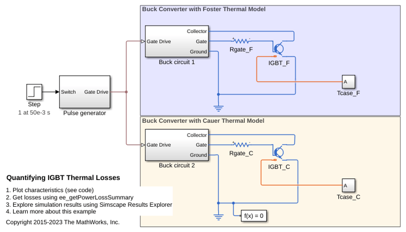
Quantifying IGBT Thermal Losses
The generation of a temperature profile based on switching and conduction losses in an insulated-gate bipolar transistor (IGBT). There are two buck converters. For one converter, the IGBT attaches to a Foster thermal model. For the other converter, the IGBT attaches to a Cauer thermal model. The parameters for the thermal models are tuned to give roughly equivalent results. At a simulation time of 50ms, the driving frequency changes from 40kHz to 20kHz, which increases the conduction losses and decreases the switching losses. The change in the losses results in a corresponding change in the temperature of the IGBT.
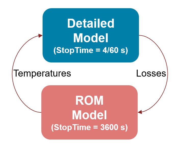
Optimize Liquid Cooling System of Inverter
Analyze the performance of a liquid cooling system for a three-phase inverter. To find the steady-state temperatures and losses, you first run detailed and reduced order models (ROM). Then you compute the optimal size of the heatsink that maximizes the inverter efficiency and minimizes the lifetime cost.
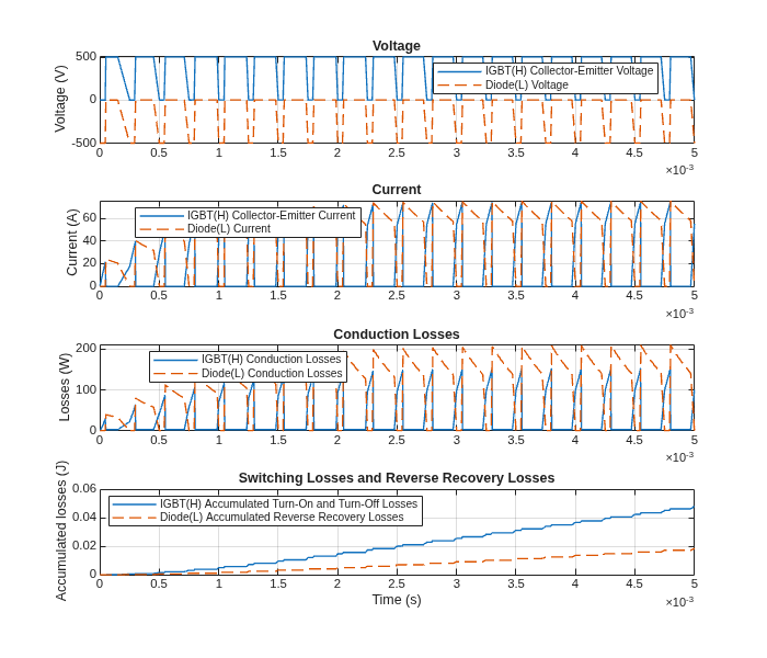
Import Infineon XML Parts into Simscape IGBT and Diode Blocks
Automatically apply parameterizations from Infineon datasheets to tabulated IGBT (Ideal, Switching) and Diode blocks in Simscape™ Electrical™.
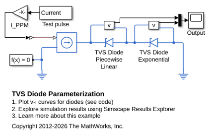
TVS Diode Parameterization
How to parameterize the Simscape™ Electrical™ diode to represent a Transient Voltage Suppression (TVS) diode. This example is for a TVS diode suited to protecting automotive electronics from voltage transients associated with turning off inductive loads. To view the data extracted from the datasheet, on the Modeling tab, in the Setup section, click Model Settings > Model Properties. On the Callbacks tab, click PreLoadFcn.
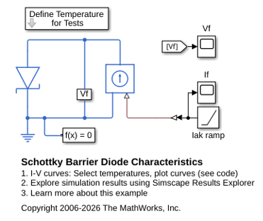
Schottky Barrier Diode Characteristics
Generation of the current versus voltage curve for a Schottky barrier diode. Define the vector of temperatures for which to plot the characteristics by double clicking on the block labeled 'Define Temperatures for Tests'. Run the tests and plot the I-V curves by clicking in the model on the hyperlink 'plot curves'.
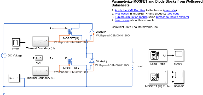
Parameterize MOSFET and Diode Blocks from Wolfspeed Datasheets
Automatically apply parameterizations from Wolfspeed® datasheets to tabulated MOSFET (Ideal, Switching) and Diode blocks in Simscape™ Electrical™.
Assumptions and Limitations
When you select
Use two I-V curve data pointsfor the Parameterization parameter, choose a pair of voltages near the diode turn-on voltage. Typically, this is in the range from 0.05 to 1 V. Using values outside of this region may lead to numerical issues and poor estimates for IS and N.The block does not account for temperature-dependent effects on the junction capacitance.
You might need to use nonzero ohmic resistance and junction capacitance values to prevent numerical simulation issues, but the simulation may run faster with these values set to zero.
If the value you specify for the Off state conductance parameter (Goff) is greater than the value of the on-state forward conductance for small forward voltages (gOnMin) that the block derives during the simulation, then the block uses the value of gOnMin to compute the reverse I-V characteristics of the diode instead of the value of the Off state conductance parameter. This assumption also applies to the faulted scenario.
The Diode block does not support energy accounting. If you try to get energy information for this block using the
getEnergyInfofunction, the function generates an error message.
Ports
Conserving
Parameters
References
[1] MH. Ahmed and P.J. Spreadbury. Analogue and digital electronics for engineers. 2nd Edition. Cambridge, UK: Cambridge University Press, 1984.
[2] G. Massobrio and P. Antognetti. Semiconductor Device Modeling with SPICE. 2nd Edition. New York: McGraw-Hill, 1993.
[3] Lauritzen, P.O. and C.L. Ma. “A Simple Diode Model with Reverse Recovery.” IEEE® Transactions on Power Electronics. Vol. 6, No. 2, April 1991, pp. 188–191.
Extended Capabilities
Version History
Introduced in R2008aSee Also
Simscape Blocks
- Ideal Semiconductor Switch | MOSFET (Ideal, Switching) | IGBT (Ideal, Switching) | GTO | Thyristor (Piecewise Linear) | Half-Bridge (Ideal, Switching) | N-Channel MOSFET | P-Channel MOSFET

