Design Pixel-Streaming Algorithms for Hardware Targeting
Hardware-targeted video processing designs use a pixel-streaming video format. Serial processing is efficient for hardware designs because less memory is required to store pixel data for computation. Vision HDL Toolbox™ blocks use a streaming pixel interface, with an accompanying control signal bus. The control signals indicate the relative location of each pixel in the image or video frame. The interface mimics the timing of a video system, including inactive intervals between frames. This protocol enables each block to operate independently of image size and format and makes the design more resilient to video timing errors. You can model single-pixel or multipixel streaming designs.
Note
The reference design on the Zynq® device requires the same video resolution and color format for the entire data path. The resolution you select on the Video Capture HDMI or Video Capture MIPI block must match that of your camera input. The Video Capture USB block automatically shows only the resolutions supported by your camera. The design you target to the user logic section of the FPGA must not modify the frame size or color space of the video stream. The input and output of the user logic must also have the same number of pixels per cycle.
Single-Pixel Streaming from MIPI Input
To get started with pixel-streaming design, begin with a model like that shown in the Corner Detection with Zynq-Based Hardware and MIPI Sensor example. The model converts the video data from frames to pixel streams and vice versa. To design an algorithm for FPGA deployment, add Vision HDL Toolbox blocks to the model.
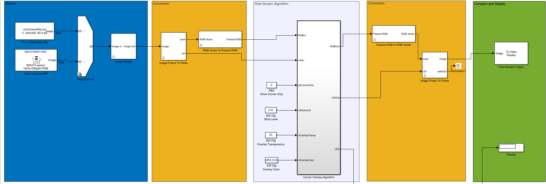
The model has five shaded areas.
Source — This area contains the video data sources for your model. The Video Capture MIPI block provides live camera data from a MIPI® card. Alternatively, you can select a file input.
Conversion (1) — The blocks in this area convert frame RGB video data into a pixel stream. The Image Frame To Pixels block maps the resolutions supported by the Video Capture MIPI block into custom timing parameters on the Frame To Pixels block (from Vision HDL Toolbox). Also, the model packs the color components as required for the AXI4-Stream Video interface and the FPGA targeting tools. The targeting tools recognize the control bus and flatten the signals in the generated HDL code. To use 2-pixel-per-clock streaming, set the Number of pixels parameter on both these blocks to
2.Algorithm — This area contains the subsystem where you design your algorithms. This subsystem can include ports for physical board signals. It can also include ports connected to AXI-Lite registers, which you can control from the ARM® processor. This algorithm can optionally connect to an AXI manager external memory interface.
Conversion (2) — The blocks in this area unpack the color components and convert the pixel stream back to frames. To use 2-pixel-per-clock streaming, set the Number of pixels parameter on both these blocks to
2.Display — This area contains the display and evaluation of the results of the video processing algorithm.
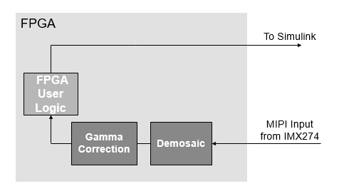
To capture video from the hardware board, the support package implements this
design on the FPGA. The FPGA user logic is programmed with your design from the
Pixel-Streaming Algorithm subsystem. In the generated HDL
code, the interface of the FPGA user logic uses an AXI4-Stream Video interface.
Single-Pixel Streaming from HDMI Input
The model templates for single-pixel-streaming algorithms can help you get started with your design. The templates convert the video data from frames to pixel streams and vice versa. To design an algorithm for FPGA deployment, add Vision HDL Toolbox blocks to the template. To open a template, see Create Model Using Simulink Templates.
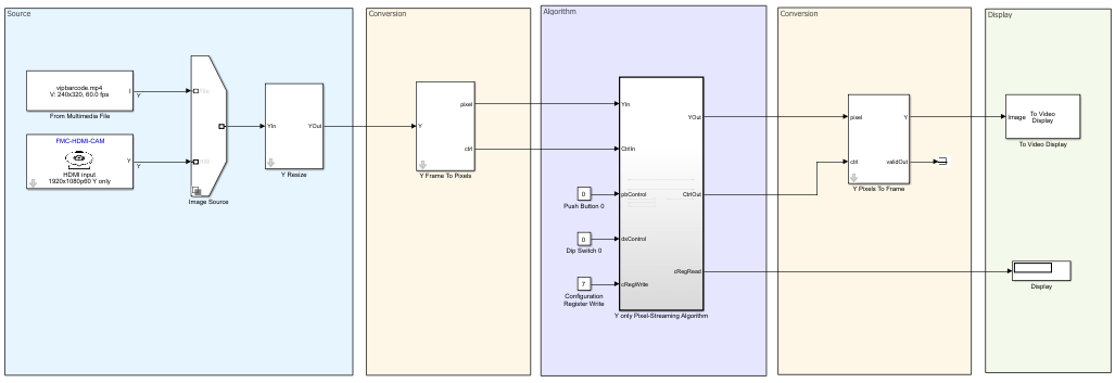
Each template has five shaded areas.
Source — This area contains the video data sources for your model. The Video Capture HDMI block provides either live camera data from an HDMI card or a test pattern from the hardware device. Alternatively, you can select data file input.
Conversion (1) — The subsystem in this area converts frame video data into a pixel stream. The Image Frame To Pixels block maps the resolutions supported by the Video Capture HDMI block into custom timing parameters on the Frame To Pixels block (from Vision HDL Toolbox). Also, the model flattens the color components as required for the FPGA-targeting tools. The targeting tools recognize the control bus and flatten the signals in the generated HDL code.
Algorithm — This area contains the subsystem where you design your algorithms. This subsystem can include ports for physical board signals. It can also include ports connected to AXI-Lite registers, which you can control from the ARM processor. This algorithm can optionally connect to external memory, such as a frame buffer.
Conversion (2) — The subsystem in this area converts the pixel stream back to frames and reconstructs the color components.
Display — This area contains the display and evaluation of the results of the video processing algorithm.
To capture video from the hardware board, the support package implements this
design on the FPGA. The FPGA user logic is programmed with your design from the
Pixel-Streaming Algorithm subsystem. Without any FPGA user
logic added to this design, the video captured from both points is identical.
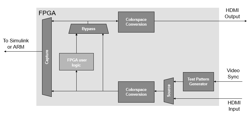
You can implement the interface of your FPGA user logic with the Vision HDL Toolbox custom streaming video interface or with an AXI4-Stream Video interface. You can select the interface implementation when you generate HDL code for the Algorithm subsystem.
Multipixel Streaming from HDMI Input
You can also model and deploy multipixel streams. These streams provide 4 or 8 pixels per cycle to support high-rate or high-resolution video. Multipixel streaming increases hardware resources to support higher video resolutions with the same hardware clock rate as a smaller resolution video.
Note
Multipixel streaming is not supported with an external memory interface, or with the AXI4-Stream Video interface.
Convert the input video to a multipixel stream by setting the Number of
pixels parameter greater than 1 in the Frame To Pixels
block in your model. This model image shows that the output signals from the block
are vectors with the number of pixels you specified for the Number of
pixels parameter. In this case, the model has an input frame signal
of size 1080-by-1920-by-3 and an output RGB pixel stream signal of size 4-by-3 from
the Frame To Pixels block. The R, G, and B signals to the
Algorithm subsystem each are of size 4-by-1.To convert the
multipixel stream back to frame format, you must also set the Number of
pixels parameter in the output Pixels To Frame
block.
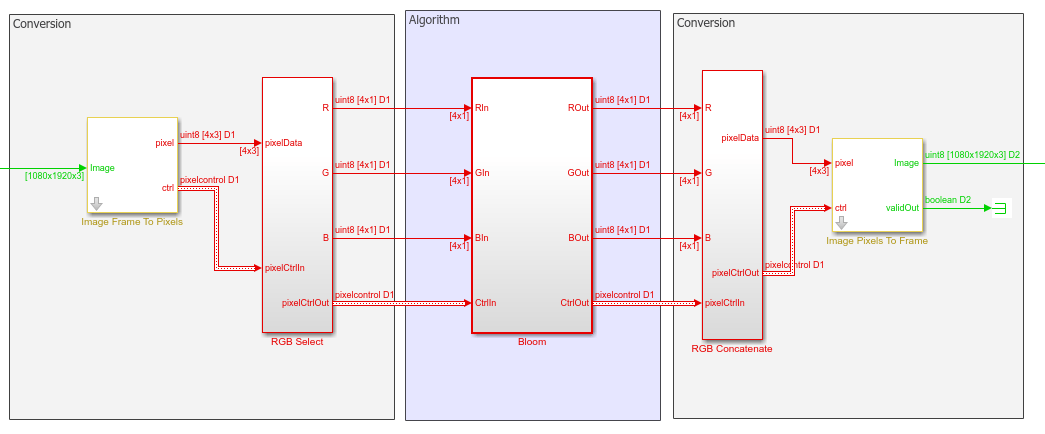
The dimensions of your video format must be multiples of the number of pixels per cycle. Specifically, Active pixels per line, Total pixels per line, Front porch, and Back porch parameters of the Frame To Pixels block must be multiples of Number of pixels.
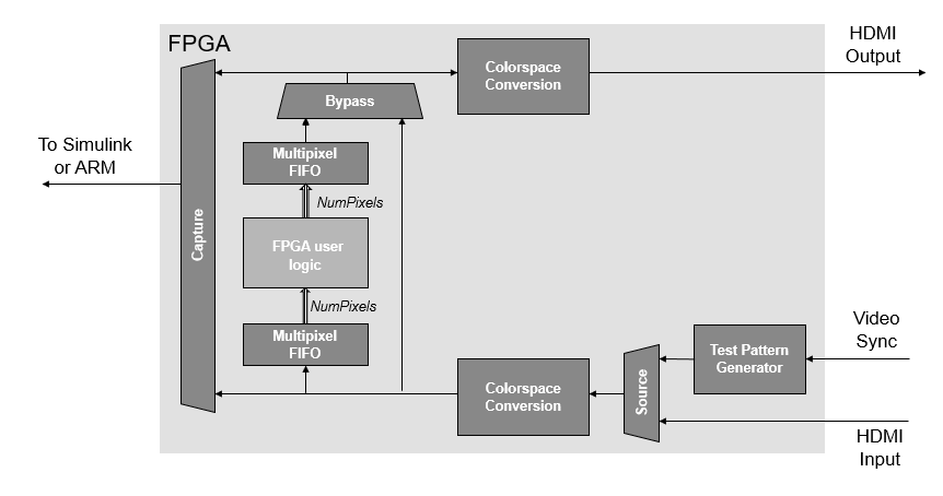
To capture video from the hardware board, the support package implements this
design on the FPGA. The FPGA user logic is programmed with your design from the
Pixel-Streaming Algorithm subsystem. If your design uses
multipixel streaming, the FPGA design includes FIFOs at the input and output of the
FPGA user logic that convert a scalar pixel stream to a multipixel stream. In the
multipixel case, the FPGA user logic runs at a clock rate of
HDMIClockRate/NumPixels.
HDMIClockRate is the speed of the clock from the HDMI
interface on the board and depends on your video resolution.
NumPixels is the value of the Number of
pixels parameter of the Frame To Pixels block.
For an example of modeling and deploying a multipixel stream design, see MultiPixel-MultiComponent Streaming with Zynq-Based Hardware.
Next Steps
When you are satisfied with the results of the video processing in Simulink®, run the HDL Workflow Advisor on the Pixel-Streaming
Algorithm subsystem to generate code and load the design to the FPGA.
For more detail, see Target FPGA on Zynq Hardware.
See Also
Video Capture HDMI | Video Capture MIPI