Triggering Software Tasks by FPGA Interrupts
This example shows how to model an algorithm partitioned between hardware and software. The hardware IP is implemented in FPGA fabric, and triggers a software task implemented in the embedded processor. Design, simulate, and implement a complete design on SoC hardware.
Supported hardware platforms:
Xilinx® Zynq® ZC706 evaluation kit
Xilinx Zynq UltraScale™+ MPSoC ZCU102 Evaluation Kit
Xilinx Zynq UltraScale+ RFSoC ZCU111 Evaluation Kit
ZedBoard™ Zynq-7000 Development Board
Altera® Cyclone® V SoC development kit
Altera Arria® 10 SoC development kit
Introduction
Many System-on-Chip (SoC) applications require the hardware device to trigger an asynchronous task on the processor. This functionality can be useful when implementing low-latency control loops that span between the hardware and software. It is also useful in handling urgent hardware requests by the software. For such designs, the hardware device raises an interrupt request to the interrupt controller to signify that data is ready for action by the software task on the processor.
Design Task
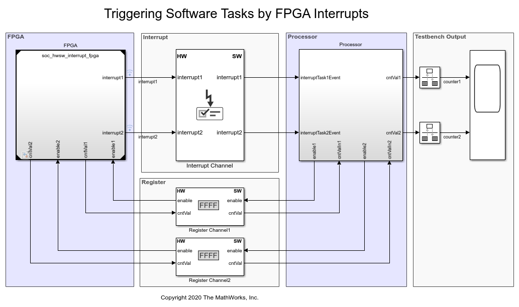
This example includes two hardware IP cores in the FPGA. These IP cores generate the interrupt signals asynchronously. The interrupts trigger two separate tasks on the processor, one for each hardware IP core. The processor tasks access the hardware devices by reading or writing registers.
Model Structure

The top model soc_hwsw_interrupt_top includes the FPGA model soc_hwsw_interrupt_fpga and processor model soc_hwsw_interrupt_proc as model references. The top model also includes the Interrupt Channel and Register Channel blocks to model data transfers from the FPGA to the Processor.

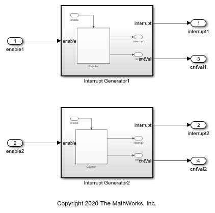
The FPGA model implements two IP cores that generate interrupts based on incrementing 32 bit-counter values. The first IP core generates an interrupt when either the 16th or the 18th bit of the counter value changes from 0 to 1. The second IP core generates an interrupt when either the 14th or 16th bit of the counter value changes from 0 to 1. The counter value at the time of generating the interrupt is registered and transferred to the processor using the Register Channel block. The processor model implements two software tasks, one for each IP core, that read the counter value, previously registered by the FPGA.

Simulation
Simulate the system for 0.03 seconds and open the Scope block on the top model to visualize the counter values as they are read by the processor.

Next, on the Simulation tab, click Data Inspector to view the timing of various events triggered by interrupts. Add interrupt1 and interruptTask1 signals in the top view, and add interrupt2 and interruptTask2 signals in the bottom view. The simulation plot shows that every time an interrupt is triggered, the corresponding task is executed. At time 0.01802 seconds, interrupt2 is raised and takes 100 microseconds to process by the Interrupt Channel block and to trigger the corresponding interruptTask2, which takes 500 microseconds to run.

At time 0.01966 seconds, interrupt1 & interrupt2 are raised at the same time, and they are serviced by the processor based on their relative priority. Since interrupt1 is connected first at the input ports of the Interrupt Channel block, it has a higher priority than interrupt2. interruptTask2 waits to be executed while interruptTask1 is still executing due to the higher priority of interrupt1.
Implement and Run on Hardware
These products are required for this section:
HDL Coder™
Embedded Coder®
SoC Blockset™ Support Package for AMD® FPGA and SoC Devices, or SoC Blockset Support Package for Intel® Devices
For more information about support packages, see SoC Blockset Supported Hardware.
To implement the model on a supported SoC board use the SoC Builder tool. In the Simulink toolstrip, on the System on Chip tab, open the Configuration Parameters window by clicking Hardware Settings. In the Configuration Parameters window, in Hardware Implementation, select board as Xilinx Zynq UltraScale+ MPSoC ZCU102 Evaluation Kit from the Hardware board list for the top and processor models. For processor model, set Processing Unit as APU under Hardware board settings. To open SoC Builder, click Configure, Build, & Deploy button in the toolstrip and follow these steps:
On the Setup screen, select Build model. Click Next.
On the Select Build Action screen, select Build and load for external mode. Click Next.
On the Select Project Folder screen, specify the project folder. Click Next.
On the Review Hardware Mapping screen, click Next.
On the Review Memory Map screen, view the memory map by clicking View/Edit. Click Next.
On the Validate Model screen, check the compatibility of the model for implementation by clicking Validate. Click Next.
On the Build Model screen, begin building the model by clicking Build. An external shell opens when FPGA synthesis begins. Click Next.
On the Connect Hardware screen, test the connectivity of the host computer with the SoC board by clicking Test Connection. To go to the Run Application screen, click Next.
The FPGA synthesis often takes more than 30 minutes to complete. To save time, you may want to use the provided pre-generated bitstream by following these steps:
Close the external shell to terminate synthesis.
Copy pregenerated bitstream to your project folder by running this
copyfilecommand below.Load pre-generated bitstream and run the model on the SoC board by clicking Load and Run.
copyfile(fullfile(matlabshared.supportpkg.getSupportPackageRoot,'toolbox','soc',...
        'supportpackages','xilinxsoc','xilinxsocexamples','bitstreams',...
        'soc_hwsw_interrupt_top-zcu102.bit'), './soc_prj');
After loading the bitstream, run the generated software model soc_hwsw_interrupt_sw in external mode. From the model toolbar, open the Data Inspector and add interruptTask1 in the top view and interruptTask2 into the bottom view. Observe that every time an interrupt is triggered the corresponding task is executed.
Implementation on other boards: To implement the model on a supported board other than ZCU102, first configure the model to the supported board, and then set the example parameters as below.
In the Simulink® toolstrip, on the System on Chip tab, open Configuration Parameters window by clicking Hardware Settings.
In the Configuration Parameters window, in Hardware Implementation, select your board from Hardware board drop-down list on both top and processor model.
In the Hardware board settings section, expand Target hardware resources. Under Groups, click FPGA design (top level). Select Include 'AXI Manager' IP for host-based interaction and specify IP core clock frequency (MHz) as
10.In the Simulink toolstrip of processor model, on the System on Chip tab, open Configuration Parameters window by clicking Hardware Settings. In the Configuration Parameters window, in Hardware Implementation, under Hardware board settings, select
APUfrom Processing Unit drop-down list.
Next, click Configure, Build, & Deploy on the toolstrip to open SoC Builder and follow the steps as previously stated for Xilinx Zynq UltraScale+ MPSoC ZCU102 evaluation kit. Generate the bitstream and load it onto the hardware board for all other Xilinx boards. Intel boards use pregenerated bitstreams. In case of Altera Arria® 10 SoC development kit and Altera Cyclone® V SoC development kit, use the below copyfile command corresponding to your board. For example, if you use a Cyclone V SoC development kit, use this command to copy the '.periph.rbf' and '.core.rbf' files.
copyfile(fullfile(matlabshared.supportpkg.getSupportPackageRoot,'toolbox','soc',...
        'supportpackages','intelsoc','intelsocexamples','bitstreams',...
        'soc_hwsw_interrupt_top-c5soc.rbf'), './soc_prj');
The following are the available pre-generated bitstream files:
'soc_hwsw_interrupt_top-zcu102.bit'
'soc_hwsw_interrupt_top-c5soc.rbf'
'soc_hwsw_interrupt_top-a10soc.periph.rbf'
'soc_hwsw_interrupt_top-a10soc.core.rbf'
In summary, this example showed how interrupts from the FPGA trigger actions in the processor. You modeled the behavior using SoC Blockset, and went through the workflow required to implement it on an SoC device.